- 您現(xiàn)在的位置:買(mǎi)賣(mài)IC網(wǎng) > PDF目錄370849 > M37902F8CHP (Mitsubishi Electric Corporation) DIODE SCHOTTKY DUAL COMMON-ANODE 25V 200mW 0.32V-vf 200mA-IFM 1mA-IF 2uA-IR SOT-23 3K/REEL PDF資料下載
參數(shù)資料
| 型號(hào): | M37902F8CHP |
| 廠商: | Mitsubishi Electric Corporation |
| 英文描述: | DIODE SCHOTTKY DUAL COMMON-ANODE 25V 200mW 0.32V-vf 200mA-IFM 1mA-IF 2uA-IR SOT-23 3K/REEL |
| 中文描述: | 單片16位CMOS微機(jī) |
| 文件頁(yè)數(shù): | 40/143頁(yè) |
| 文件大小: | 1463K |
| 代理商: | M37902F8CHP |
第1頁(yè)第2頁(yè)第3頁(yè)第4頁(yè)第5頁(yè)第6頁(yè)第7頁(yè)第8頁(yè)第9頁(yè)第10頁(yè)第11頁(yè)第12頁(yè)第13頁(yè)第14頁(yè)第15頁(yè)第16頁(yè)第17頁(yè)第18頁(yè)第19頁(yè)第20頁(yè)第21頁(yè)第22頁(yè)第23頁(yè)第24頁(yè)第25頁(yè)第26頁(yè)第27頁(yè)第28頁(yè)第29頁(yè)第30頁(yè)第31頁(yè)第32頁(yè)第33頁(yè)第34頁(yè)第35頁(yè)第36頁(yè)第37頁(yè)第38頁(yè)第39頁(yè)當(dāng)前第40頁(yè)第41頁(yè)第42頁(yè)第43頁(yè)第44頁(yè)第45頁(yè)第46頁(yè)第47頁(yè)第48頁(yè)第49頁(yè)第50頁(yè)第51頁(yè)第52頁(yè)第53頁(yè)第54頁(yè)第55頁(yè)第56頁(yè)第57頁(yè)第58頁(yè)第59頁(yè)第60頁(yè)第61頁(yè)第62頁(yè)第63頁(yè)第64頁(yè)第65頁(yè)第66頁(yè)第67頁(yè)第68頁(yè)第69頁(yè)第70頁(yè)第71頁(yè)第72頁(yè)第73頁(yè)第74頁(yè)第75頁(yè)第76頁(yè)第77頁(yè)第78頁(yè)第79頁(yè)第80頁(yè)第81頁(yè)第82頁(yè)第83頁(yè)第84頁(yè)第85頁(yè)第86頁(yè)第87頁(yè)第88頁(yè)第89頁(yè)第90頁(yè)第91頁(yè)第92頁(yè)第93頁(yè)第94頁(yè)第95頁(yè)第96頁(yè)第97頁(yè)第98頁(yè)第99頁(yè)第100頁(yè)第101頁(yè)第102頁(yè)第103頁(yè)第104頁(yè)第105頁(yè)第106頁(yè)第107頁(yè)第108頁(yè)第109頁(yè)第110頁(yè)第111頁(yè)第112頁(yè)第113頁(yè)第114頁(yè)第115頁(yè)第116頁(yè)第117頁(yè)第118頁(yè)第119頁(yè)第120頁(yè)第121頁(yè)第122頁(yè)第123頁(yè)第124頁(yè)第125頁(yè)第126頁(yè)第127頁(yè)第128頁(yè)第129頁(yè)第130頁(yè)第131頁(yè)第132頁(yè)第133頁(yè)第134頁(yè)第135頁(yè)第136頁(yè)第137頁(yè)第138頁(yè)第139頁(yè)第140頁(yè)第141頁(yè)第142頁(yè)第143頁(yè)
M37902FCCHP, M37902FGCHP, M37902FJCHP
SINGLE-CHIP 16-BIT CMOS MICROCOMPUTER
MITSUBISHI MICROCOMPUTERS
40
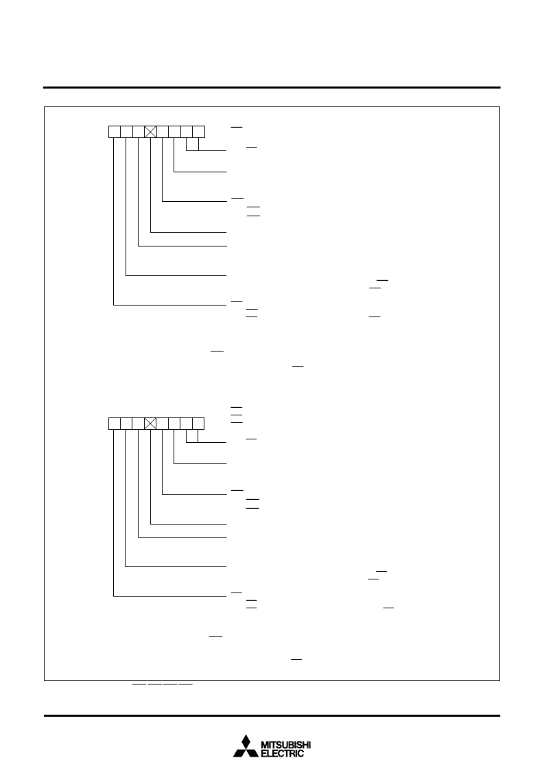
Fig. 28 Bit configuration of CS
0
/CS
1
/CS
2
/CS
3
control register Ls
7
6
5
4
3
2
1
0
CS
0
control register L
External data bus width select bit
(Note 1)
0 : 16-bit width
1 : 8-bit width
RDY control bit
(Note 2)
0 : RDY control is valid.
1 : RDY control is invalid.
Area CS
0
bus cycle select bit 0
See Figure 18.
Address
80
16
At reset
42
16
Burst ROM access select bit
(Note 3)
0 : Normal access
1 : Burst ROM access
Recovery cycle insert select bit
0 : No recovery cycle is inserted at access to area CS
0
.
1 : Recovery cycle is inserted at access to area CS
0
.
CS
0
output select bit
(Notes 4, 5)
0 : CS
0
output is disabled. (P4
4
functions as a programmble I/O port pin.)
1 : CS
0
output is enabled. (P4
4
functions as pin CS
0
.)
Notes 1:
While V
SS
level voltage is applied to pin BYTE, this bit
’
s state is cleared to
“
0
”
at reset. While V
CC
level voltage is
applied to pin BYTE, on the other hand, this bit
’
s state is set to
“
1
”
at reset.
2:
This bit is valid when the RDY input select bit (bit 2 at address 5F
16
) =
“
1
”
.
3:
While V
CC
level voltage is applied to pin BYTE, the normal access is selected regardless of this bit
’
s contents.
4:
In the single-chip mode, this bit
’
s contents are invalid. (CS
0
output is disabled.)
5:
While V
SS
level voltage is applied to pin MD0, this bit
’
s state is cleared to
“
0
”
at reset. While V
CC
level voltage is
applied to pin MD0, on the other hand, this bit
’
s state is set to
“
1
”
at reset. (Fixed to
“
1
”
.)
7
6
5
4
3
2
1
0
CS
1
control register L
CS
2
control register L
CS
3
control register L
External data bus width select bit
0 : 16-bit width
1 : 8-bit width
(Note 1)
RDY control bit
(Note 2)
0 : RDY control is valid.
1 : RDY control is invalid.
Area CS
j
bus cycle select bit 0 (j = 1 to 3)
See Figure 18.
“
0
”
at reading.
Address
82
16
84
16
86
16
At reset
42
16
42
16
42
16
Burst ROM access select bit
(Note 3)
0 : Normal access
1 : Burst ROM access
Recovery cycle insert select bit
0 : No recovery cycle is inserted at access to area CS
j
.
1 : Recovery cycle is inserted at access to area CS
j
.
CS
j
output select bit (j = 1 to 3)
(Note 4)
0 : CS
j
output is disabled. (P4
5
to P4
7
function as programmable I/O port pins.)
1 : CS
j
output is enabled. (P4
5
to P4
7
function as pin CS
j
.)
Notes 1:
While V
CC
level voltage is applied to pin BYTE, this bit is fixed to
“
1
”
(8-bit width).
2:
This bit is valid when the RDY input select bit (bit 2 at address 5F
16
) =
“
1
”
.
3:
When only the external data bus width select bit (bit 2) =
“
1
”
or while V
CC
level voltage is applied to pin BYTE, the
normal access is selected regardless of this bit
’
s contents.
4:
In the single-chip mode, this bit
’
s contents are invalid. (CS
0
output is disabled.)
“
0
”
at read.
相關(guān)PDF資料 |
PDF描述 |
|---|---|
| M37902FGCGP | SINGLE-CHIP 16-BIT CMOS MICROCOMPUTER |
| M37902FCCHP | SINGLE-CHIP 16-BIT CMOS MICROCOMPUTER |
| M37902FGCHP | DIODE SCHOTTKY DUAL COMMON-ANODE 25V 150mW 0.32V-vf 200mA-IFM 1mA-IF 2uA-IR SOT-523 3K/REEL |
| M37902FJCHP | SINGLE-CHIP 16-BIT CMOS MICROCOMPUTER |
| M37905F8CFP | 16-BIT CMOS MICROCOMPUTER |
相關(guān)代理商/技術(shù)參數(shù) |
參數(shù)描述 |
|---|---|
| M37902FCCHP | 制造商:MITSUBISHI 制造商全稱(chēng):Mitsubishi Electric Semiconductor 功能描述:SINGLE-CHIP 16-BIT CMOS MICROCOMPUTER |
| M37902FGCGP | 制造商:MITSUBISHI 制造商全稱(chēng):Mitsubishi Electric Semiconductor 功能描述:SINGLE-CHIP 16-BIT CMOS MICROCOMPUTER |
| M37902FGCHP | 制造商:MITSUBISHI 制造商全稱(chēng):Mitsubishi Electric Semiconductor 功能描述:SINGLE-CHIP 16-BIT CMOS MICROCOMPUTER |
| M37902FJCHP | 制造商:MITSUBISHI 制造商全稱(chēng):Mitsubishi Electric Semiconductor 功能描述:SINGLE-CHIP 16-BIT CMOS MICROCOMPUTER |
| M37903S4CHP | 制造商:RENESAS 制造商全稱(chēng):Renesas Technology Corp 功能描述:16-BIT CMOS MICROCOMPUTER |
發(fā)布緊急采購(gòu),3分鐘左右您將得到回復(fù)。