- 您現(xiàn)在的位置:買賣IC網(wǎng) > PDF目錄299403 > LFE2-12SE-6FN256I (LATTICE SEMICONDUCTOR CORP) PDF資料下載
參數(shù)資料
| 型號(hào): | LFE2-12SE-6FN256I |
| 廠商: | LATTICE SEMICONDUCTOR CORP |
| 元件分類: | FPGA |
| 中文描述: | FPGA, 357 MHz, PBGA256 |
| 封裝: | 17 X 17 MM, LEAD FREE, FPBGA-256 |
| 文件頁數(shù): | 5/386頁 |
| 文件大小: | 3838K |
| 代理商: | LFE2-12SE-6FN256I |
第1頁第2頁第3頁第4頁當(dāng)前第5頁第6頁第7頁第8頁第9頁第10頁第11頁第12頁第13頁第14頁第15頁第16頁第17頁第18頁第19頁第20頁第21頁第22頁第23頁第24頁第25頁第26頁第27頁第28頁第29頁第30頁第31頁第32頁第33頁第34頁第35頁第36頁第37頁第38頁第39頁第40頁第41頁第42頁第43頁第44頁第45頁第46頁第47頁第48頁第49頁第50頁第51頁第52頁第53頁第54頁第55頁第56頁第57頁第58頁第59頁第60頁第61頁第62頁第63頁第64頁第65頁第66頁第67頁第68頁第69頁第70頁第71頁第72頁第73頁第74頁第75頁第76頁第77頁第78頁第79頁第80頁第81頁第82頁第83頁第84頁第85頁第86頁第87頁第88頁第89頁第90頁第91頁第92頁第93頁第94頁第95頁第96頁第97頁第98頁第99頁第100頁第101頁第102頁第103頁第104頁第105頁第106頁第107頁第108頁第109頁第110頁第111頁第112頁第113頁第114頁第115頁第116頁第117頁第118頁第119頁第120頁第121頁第122頁第123頁第124頁第125頁第126頁第127頁第128頁第129頁第130頁第131頁第132頁第133頁第134頁第135頁第136頁第137頁第138頁第139頁第140頁第141頁第142頁第143頁第144頁第145頁第146頁第147頁第148頁第149頁第150頁第151頁第152頁第153頁第154頁第155頁第156頁第157頁第158頁第159頁第160頁第161頁第162頁第163頁第164頁第165頁第166頁第167頁第168頁第169頁第170頁第171頁第172頁第173頁第174頁第175頁第176頁第177頁第178頁第179頁第180頁第181頁第182頁第183頁第184頁第185頁第186頁第187頁第188頁第189頁第190頁第191頁第192頁第193頁第194頁第195頁第196頁第197頁第198頁第199頁第200頁第201頁第202頁第203頁第204頁第205頁第206頁第207頁第208頁第209頁第210頁第211頁第212頁第213頁第214頁第215頁第216頁第217頁第218頁第219頁第220頁第221頁第222頁第223頁第224頁第225頁第226頁第227頁第228頁第229頁第230頁第231頁第232頁第233頁第234頁第235頁第236頁第237頁第238頁第239頁第240頁第241頁第242頁第243頁第244頁第245頁第246頁第247頁第248頁第249頁第250頁第251頁第252頁第253頁第254頁第255頁第256頁第257頁第258頁第259頁第260頁第261頁第262頁第263頁第264頁第265頁第266頁第267頁第268頁第269頁第270頁第271頁第272頁第273頁第274頁第275頁第276頁第277頁第278頁第279頁第280頁第281頁第282頁第283頁第284頁第285頁第286頁第287頁第288頁第289頁第290頁第291頁第292頁第293頁第294頁第295頁第296頁第297頁第298頁第299頁第300頁第301頁第302頁第303頁第304頁第305頁第306頁第307頁第308頁第309頁第310頁第311頁第312頁第313頁第314頁第315頁第316頁第317頁第318頁第319頁第320頁第321頁第322頁第323頁第324頁第325頁第326頁第327頁第328頁第329頁第330頁第331頁第332頁第333頁第334頁第335頁第336頁第337頁第338頁第339頁第340頁第341頁第342頁第343頁第344頁第345頁第346頁第347頁第348頁第349頁第350頁第351頁第352頁第353頁第354頁第355頁第356頁第357頁第358頁第359頁第360頁第361頁第362頁第363頁第364頁第365頁第366頁第367頁第368頁第369頁第370頁第371頁第372頁第373頁第374頁第375頁第376頁第377頁第378頁第379頁第380頁第381頁第382頁第383頁第384頁第385頁第386頁
www.latticesemi.com
4-1
DS1006 Pinout Information_01.9
August 2008
Data Sheet DS1006
2008 Lattice Semiconductor Corp. All Lattice trademarks, registered trademarks, patents, and disclaimers are as listed at www.latticesemi.com/legal. All other brand
or product names are trademarks or registered trademarks of their respective holders. The specications and information herein are subject to change without notice.
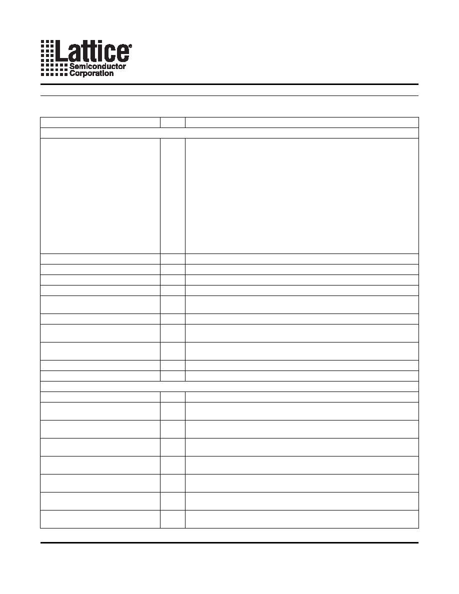
Signal Descriptions
Signal Name
I/O
Description
General Purpose
P[Edge] [Row/Column Number*]_[A/B]
I/O
[Edge] indicates the edge of the device on which the pad is located. Valid
edge designations are L (Left), B (Bottom), R (Right), T (Top).
[Row/Column Number] indicates the PFU row or the column of the device on
which the PIC exists. When Edge is T (Top) or B (Bottom), only need to spec-
ify Row Number. When Edge is L (Left) or R (Right), only need to specify Col-
umn Number.
[A/B] indicates the PIO within the PIC to which the pad is connected. Some of
these user-programmable pins are shared with special function pins. These
pins, when not used as special purpose pins, can be programmed as I/Os for
user logic. During conguration the user-programmable I/Os are tri-stated
with an internal pull-up resistor enabled. If any pin is not used (or not bonded
to a package pin), it is also tri-stated with an internal pull-up resistor enabled
after conguration.
GSRN
I
Global RESET signal (active low). Any I/O pin can be GSRN.
NC
—
No connect.
GND
—
Ground. Dedicated pins.
VCC
—
Power supply pins for core logic. Dedicated pins.
VCCAUX
—
Auxiliary power supply pin. This dedicated pin powers all the differential and
referenced input buffers.
VCCIOx
—
Dedicated power supply pins for I/O bank x.
VCCPLL
—
PLL supply pins. Should be tied to VCC even when the corresponding PLL is
unused.
VREF1_x, VREF2_x
—
Reference supply pins for I/O bank x. Pre-determined pins in each bank are
assigned as VREF inputs. When not used, they may be used as I/O pins.
XRES
4
—
10K ohm +/-1% resistor must be connected between this pad and ground.
PLLCAP
4
—
External capacitor connection for PLL.
PLL, DLL and Clock Functions (Used as user programmable I/O pins when not in use for PLL or clock pins)
[LOC][num]_VCCPLL
—
Power supply pin for PLL: ULM, LLM, URM, LRM, num = row from center.
[LOC][num]_GPLL[T, C]_IN_A
I
General Purpose PLL (GPLL) input pads: ULM, LLM, URM, LRM, num = row
from center, T = true and C = complement, index A,B,C...at each side.
[LOC][num]_GPLL[T, C]_FB_A
I
Optional feedback GPLL input pads: ULM, LLM, URM, LRM, num = row from
center, T = true and C = complement, index A,B,C...at each side.
[LOC][num]_SPLL[T, C]_IN_A
I
Secondary PLL (SPLL) input pads: ULM, LLM, URM, LRM, num = row from
center, T = true and C = complement, index A,B,C...at each side.
[LOC][num]_SPLL[T, C]_FB_A
I
Optional feedback (SPLL) input pads: ULM, LLM, URM, LRM, num = row
from center, T = true and C = complement, index A,B,C...at each side.
[LOC][num]_DLL[T, C]_IN_A
I
DLL input pads: ULM, LLM, URM, LRM, num = row from center, T = true and
C = complement, index A,B,C...at each side.
[LOC][num]_DLL[T, C]_FB_A
I
Optional feedback (DLL) input pads: ULM, LLM, URM, LRM, num = row from
center, T = true and C = complement, index A,B,C...at each side.
PCLK[T, C]_[n:0]_[3:0]
I
Primary Clock pads, T = true and C = complement, n per side, indexed by
bank and 0,1,2,3 within bank.
LatticeECP2/M Family Data Sheet
Pinout Information
相關(guān)PDF資料 |
PDF描述 |
|---|---|
| LFSCM3GA80EP1-6FCN1704C | |
| LFSC3GA15E-6FN256I | |
| LFSCM3GA40EP1-5FFN1020I | |
| LFXP2-40E-6FN484I | |
| LFXP2-17E-7F484C | |
相關(guān)代理商/技術(shù)參數(shù) |
參數(shù)描述 |
|---|---|
| LFE212SE-6FN256I | 制造商:LATTICE 制造商全稱:Lattice Semiconductor 功能描述:LatticeECP2/M Family Data Sheet |
| LFE2-12SE-6FN484C | 功能描述:FPGA - 現(xiàn)場可編程門陣列 12K LUTs S-Series 1.1.2V -6 Spd RoHS:否 制造商:Altera Corporation 系列:Cyclone V E 柵極數(shù)量: 邏輯塊數(shù)量:943 內(nèi)嵌式塊RAM - EBR:1956 kbit 輸入/輸出端數(shù)量:128 最大工作頻率:800 MHz 工作電源電壓:1.1 V 最大工作溫度:+ 70 C 安裝風(fēng)格:SMD/SMT 封裝 / 箱體:FBGA-256 |
| LFE212SE-6FN484C | 制造商:LATTICE 制造商全稱:Lattice Semiconductor 功能描述:LatticeECP2/M Family Data Sheet |
| LFE2-12SE-6FN484I | 功能描述:FPGA - 現(xiàn)場可編程門陣列 12K LUTs S-Ser 1.2V -6 Spd I RoHS:否 制造商:Altera Corporation 系列:Cyclone V E 柵極數(shù)量: 邏輯塊數(shù)量:943 內(nèi)嵌式塊RAM - EBR:1956 kbit 輸入/輸出端數(shù)量:128 最大工作頻率:800 MHz 工作電源電壓:1.1 V 最大工作溫度:+ 70 C 安裝風(fēng)格:SMD/SMT 封裝 / 箱體:FBGA-256 |
| LFE212SE-6FN484I | 制造商:LATTICE 制造商全稱:Lattice Semiconductor 功能描述:LatticeECP2/M Family Data Sheet |
發(fā)布緊急采購,3分鐘左右您將得到回復(fù)。