- 您現(xiàn)在的位置:買賣IC網(wǎng) > PDF目錄299403 > LFE2-12SE-6FN256I (LATTICE SEMICONDUCTOR CORP) PDF資料下載
參數(shù)資料
| 型號(hào): | LFE2-12SE-6FN256I |
| 廠商: | LATTICE SEMICONDUCTOR CORP |
| 元件分類: | FPGA |
| 中文描述: | FPGA, 357 MHz, PBGA256 |
| 封裝: | 17 X 17 MM, LEAD FREE, FPBGA-256 |
| 文件頁(yè)數(shù): | 333/386頁(yè) |
| 文件大小: | 3838K |
| 代理商: | LFE2-12SE-6FN256I |
第1頁(yè)第2頁(yè)第3頁(yè)第4頁(yè)第5頁(yè)第6頁(yè)第7頁(yè)第8頁(yè)第9頁(yè)第10頁(yè)第11頁(yè)第12頁(yè)第13頁(yè)第14頁(yè)第15頁(yè)第16頁(yè)第17頁(yè)第18頁(yè)第19頁(yè)第20頁(yè)第21頁(yè)第22頁(yè)第23頁(yè)第24頁(yè)第25頁(yè)第26頁(yè)第27頁(yè)第28頁(yè)第29頁(yè)第30頁(yè)第31頁(yè)第32頁(yè)第33頁(yè)第34頁(yè)第35頁(yè)第36頁(yè)第37頁(yè)第38頁(yè)第39頁(yè)第40頁(yè)第41頁(yè)第42頁(yè)第43頁(yè)第44頁(yè)第45頁(yè)第46頁(yè)第47頁(yè)第48頁(yè)第49頁(yè)第50頁(yè)第51頁(yè)第52頁(yè)第53頁(yè)第54頁(yè)第55頁(yè)第56頁(yè)第57頁(yè)第58頁(yè)第59頁(yè)第60頁(yè)第61頁(yè)第62頁(yè)第63頁(yè)第64頁(yè)第65頁(yè)第66頁(yè)第67頁(yè)第68頁(yè)第69頁(yè)第70頁(yè)第71頁(yè)第72頁(yè)第73頁(yè)第74頁(yè)第75頁(yè)第76頁(yè)第77頁(yè)第78頁(yè)第79頁(yè)第80頁(yè)第81頁(yè)第82頁(yè)第83頁(yè)第84頁(yè)第85頁(yè)第86頁(yè)第87頁(yè)第88頁(yè)第89頁(yè)第90頁(yè)第91頁(yè)第92頁(yè)第93頁(yè)第94頁(yè)第95頁(yè)第96頁(yè)第97頁(yè)第98頁(yè)第99頁(yè)第100頁(yè)第101頁(yè)第102頁(yè)第103頁(yè)第104頁(yè)第105頁(yè)第106頁(yè)第107頁(yè)第108頁(yè)第109頁(yè)第110頁(yè)第111頁(yè)第112頁(yè)第113頁(yè)第114頁(yè)第115頁(yè)第116頁(yè)第117頁(yè)第118頁(yè)第119頁(yè)第120頁(yè)第121頁(yè)第122頁(yè)第123頁(yè)第124頁(yè)第125頁(yè)第126頁(yè)第127頁(yè)第128頁(yè)第129頁(yè)第130頁(yè)第131頁(yè)第132頁(yè)第133頁(yè)第134頁(yè)第135頁(yè)第136頁(yè)第137頁(yè)第138頁(yè)第139頁(yè)第140頁(yè)第141頁(yè)第142頁(yè)第143頁(yè)第144頁(yè)第145頁(yè)第146頁(yè)第147頁(yè)第148頁(yè)第149頁(yè)第150頁(yè)第151頁(yè)第152頁(yè)第153頁(yè)第154頁(yè)第155頁(yè)第156頁(yè)第157頁(yè)第158頁(yè)第159頁(yè)第160頁(yè)第161頁(yè)第162頁(yè)第163頁(yè)第164頁(yè)第165頁(yè)第166頁(yè)第167頁(yè)第168頁(yè)第169頁(yè)第170頁(yè)第171頁(yè)第172頁(yè)第173頁(yè)第174頁(yè)第175頁(yè)第176頁(yè)第177頁(yè)第178頁(yè)第179頁(yè)第180頁(yè)第181頁(yè)第182頁(yè)第183頁(yè)第184頁(yè)第185頁(yè)第186頁(yè)第187頁(yè)第188頁(yè)第189頁(yè)第190頁(yè)第191頁(yè)第192頁(yè)第193頁(yè)第194頁(yè)第195頁(yè)第196頁(yè)第197頁(yè)第198頁(yè)第199頁(yè)第200頁(yè)第201頁(yè)第202頁(yè)第203頁(yè)第204頁(yè)第205頁(yè)第206頁(yè)第207頁(yè)第208頁(yè)第209頁(yè)第210頁(yè)第211頁(yè)第212頁(yè)第213頁(yè)第214頁(yè)第215頁(yè)第216頁(yè)第217頁(yè)第218頁(yè)第219頁(yè)第220頁(yè)第221頁(yè)第222頁(yè)第223頁(yè)第224頁(yè)第225頁(yè)第226頁(yè)第227頁(yè)第228頁(yè)第229頁(yè)第230頁(yè)第231頁(yè)第232頁(yè)第233頁(yè)第234頁(yè)第235頁(yè)第236頁(yè)第237頁(yè)第238頁(yè)第239頁(yè)第240頁(yè)第241頁(yè)第242頁(yè)第243頁(yè)第244頁(yè)第245頁(yè)第246頁(yè)第247頁(yè)第248頁(yè)第249頁(yè)第250頁(yè)第251頁(yè)第252頁(yè)第253頁(yè)第254頁(yè)第255頁(yè)第256頁(yè)第257頁(yè)第258頁(yè)第259頁(yè)第260頁(yè)第261頁(yè)第262頁(yè)第263頁(yè)第264頁(yè)第265頁(yè)第266頁(yè)第267頁(yè)第268頁(yè)第269頁(yè)第270頁(yè)第271頁(yè)第272頁(yè)第273頁(yè)第274頁(yè)第275頁(yè)第276頁(yè)第277頁(yè)第278頁(yè)第279頁(yè)第280頁(yè)第281頁(yè)第282頁(yè)第283頁(yè)第284頁(yè)第285頁(yè)第286頁(yè)第287頁(yè)第288頁(yè)第289頁(yè)第290頁(yè)第291頁(yè)第292頁(yè)第293頁(yè)第294頁(yè)第295頁(yè)第296頁(yè)第297頁(yè)第298頁(yè)第299頁(yè)第300頁(yè)第301頁(yè)第302頁(yè)第303頁(yè)第304頁(yè)第305頁(yè)第306頁(yè)第307頁(yè)第308頁(yè)第309頁(yè)第310頁(yè)第311頁(yè)第312頁(yè)第313頁(yè)第314頁(yè)第315頁(yè)第316頁(yè)第317頁(yè)第318頁(yè)第319頁(yè)第320頁(yè)第321頁(yè)第322頁(yè)第323頁(yè)第324頁(yè)第325頁(yè)第326頁(yè)第327頁(yè)第328頁(yè)第329頁(yè)第330頁(yè)第331頁(yè)第332頁(yè)當(dāng)前第333頁(yè)第334頁(yè)第335頁(yè)第336頁(yè)第337頁(yè)第338頁(yè)第339頁(yè)第340頁(yè)第341頁(yè)第342頁(yè)第343頁(yè)第344頁(yè)第345頁(yè)第346頁(yè)第347頁(yè)第348頁(yè)第349頁(yè)第350頁(yè)第351頁(yè)第352頁(yè)第353頁(yè)第354頁(yè)第355頁(yè)第356頁(yè)第357頁(yè)第358頁(yè)第359頁(yè)第360頁(yè)第361頁(yè)第362頁(yè)第363頁(yè)第364頁(yè)第365頁(yè)第366頁(yè)第367頁(yè)第368頁(yè)第369頁(yè)第370頁(yè)第371頁(yè)第372頁(yè)第373頁(yè)第374頁(yè)第375頁(yè)第376頁(yè)第377頁(yè)第378頁(yè)第379頁(yè)第380頁(yè)第381頁(yè)第382頁(yè)第383頁(yè)第384頁(yè)第385頁(yè)第386頁(yè)
2-47
Architecture
Lattice Semiconductor
LatticeECP2/M Family Data Sheet
Each Transmit and Receive channel has its independent power supplies. The Output and Input buffers of each
channel also have their own independent power supplies. In addition, there are separate power supplies for PLL,
terminating resistor per quad.
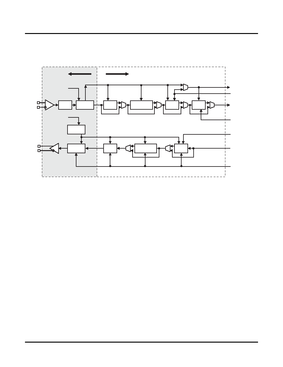
Figure 2-40. Simplied Channel Block Diagram for SERDES and PCS
PCS
As shown in Figure 2-40, the PCS receives the parallel digital data from the deserializer receivers and adjusts the
polarity, detects, byte boundary, decodes (8b/10b) and provides Clock Tolerance Compensation (CTC) FIFO for
changing the clock domain from receiver clock to the FPGA Clock.
For the transmit channel, the PCS block receives the parallel data from the FPGA core, encodes it with 8b/10b,
adjusts the polarity and passes the 8/10 bit data to the transmit SERDES channel.
The PCS also provides bypass modes that allow a direct 8-bit or 10-bit interface from the SERDES to the FPGA
logic. The PCS interface to FPGA can also be programmed to run at 1/2 speed for a 16-bit or 20-bit interface to the
FPGA logic.
SCI (SERDES Client Interface) Bus
The SERDES Client Interface (SCI) is a soft IP interface that allow the SERDES/PCS Quad block to be controlled
by registers as opposed to the conguration memory cells. It is a simple register conguration interface.
The ispLEVER design tools from Lattice support all modes of the PCS. Most modes are dedicated to applications
associated with a specic industry standard data protocol. Other more general purpose modes allow users to
dene their own operation. With ispLEVER, the user can dene the mode for each quad in a design.
Popular standards such as 10Gb Ethernet and x4 PCI-Express and 4x Serial RapidIO can be implemented using
IP (provided by Lattice), a single quad (Four SERDES channels and PCS) and some additional logic from the core.
For further information about SERDES, please see the list of additional technical documentation at the end of this
data sheet.
Deserializer
1:8/1:10
Polarity
Adjust
Equalizer
Byte Boundary
Detect, 8b/10b
Decoder
CTC
FIFO
Down
Sample
FIFO
Up
Sample
FIFO
8b/10b
Encoder
Polarity
Adjust
Serializer
TX PLL
FPGA Transmit Clock
Recovered Clock
RX REFCLK
FPGA Receive Clock
To FPGA Core
Transmit
Receiver
8/10 bits or
16/20 bits
Transmit Data
Elastic Buffer
Read Clock
16/20 bits
Receive Data
From Transmit PLL
(In Common Block)
SERDES (Analog)
PCS (Digital)
8:1/10:1
TX REFCLK
相關(guān)PDF資料 |
PDF描述 |
|---|---|
| LFSCM3GA80EP1-6FCN1704C | |
| LFSC3GA15E-6FN256I | |
| LFSCM3GA40EP1-5FFN1020I | |
| LFXP2-40E-6FN484I | |
| LFXP2-17E-7F484C | |
相關(guān)代理商/技術(shù)參數(shù) |
參數(shù)描述 |
|---|---|
| LFE212SE-6FN256I | 制造商:LATTICE 制造商全稱:Lattice Semiconductor 功能描述:LatticeECP2/M Family Data Sheet |
| LFE2-12SE-6FN484C | 功能描述:FPGA - 現(xiàn)場(chǎng)可編程門陣列 12K LUTs S-Series 1.1.2V -6 Spd RoHS:否 制造商:Altera Corporation 系列:Cyclone V E 柵極數(shù)量: 邏輯塊數(shù)量:943 內(nèi)嵌式塊RAM - EBR:1956 kbit 輸入/輸出端數(shù)量:128 最大工作頻率:800 MHz 工作電源電壓:1.1 V 最大工作溫度:+ 70 C 安裝風(fēng)格:SMD/SMT 封裝 / 箱體:FBGA-256 |
| LFE212SE-6FN484C | 制造商:LATTICE 制造商全稱:Lattice Semiconductor 功能描述:LatticeECP2/M Family Data Sheet |
| LFE2-12SE-6FN484I | 功能描述:FPGA - 現(xiàn)場(chǎng)可編程門陣列 12K LUTs S-Ser 1.2V -6 Spd I RoHS:否 制造商:Altera Corporation 系列:Cyclone V E 柵極數(shù)量: 邏輯塊數(shù)量:943 內(nèi)嵌式塊RAM - EBR:1956 kbit 輸入/輸出端數(shù)量:128 最大工作頻率:800 MHz 工作電源電壓:1.1 V 最大工作溫度:+ 70 C 安裝風(fēng)格:SMD/SMT 封裝 / 箱體:FBGA-256 |
| LFE212SE-6FN484I | 制造商:LATTICE 制造商全稱:Lattice Semiconductor 功能描述:LatticeECP2/M Family Data Sheet |
發(fā)布緊急采購(gòu),3分鐘左右您將得到回復(fù)。