- 您現(xiàn)在的位置:買賣IC網(wǎng) > PDF目錄299403 > LFE2-12SE-6FN256I (LATTICE SEMICONDUCTOR CORP) PDF資料下載
參數(shù)資料
| 型號: | LFE2-12SE-6FN256I |
| 廠商: | LATTICE SEMICONDUCTOR CORP |
| 元件分類: | FPGA |
| 中文描述: | FPGA, 357 MHz, PBGA256 |
| 封裝: | 17 X 17 MM, LEAD FREE, FPBGA-256 |
| 文件頁數(shù): | 268/386頁 |
| 文件大小: | 3838K |
| 代理商: | LFE2-12SE-6FN256I |
第1頁第2頁第3頁第4頁第5頁第6頁第7頁第8頁第9頁第10頁第11頁第12頁第13頁第14頁第15頁第16頁第17頁第18頁第19頁第20頁第21頁第22頁第23頁第24頁第25頁第26頁第27頁第28頁第29頁第30頁第31頁第32頁第33頁第34頁第35頁第36頁第37頁第38頁第39頁第40頁第41頁第42頁第43頁第44頁第45頁第46頁第47頁第48頁第49頁第50頁第51頁第52頁第53頁第54頁第55頁第56頁第57頁第58頁第59頁第60頁第61頁第62頁第63頁第64頁第65頁第66頁第67頁第68頁第69頁第70頁第71頁第72頁第73頁第74頁第75頁第76頁第77頁第78頁第79頁第80頁第81頁第82頁第83頁第84頁第85頁第86頁第87頁第88頁第89頁第90頁第91頁第92頁第93頁第94頁第95頁第96頁第97頁第98頁第99頁第100頁第101頁第102頁第103頁第104頁第105頁第106頁第107頁第108頁第109頁第110頁第111頁第112頁第113頁第114頁第115頁第116頁第117頁第118頁第119頁第120頁第121頁第122頁第123頁第124頁第125頁第126頁第127頁第128頁第129頁第130頁第131頁第132頁第133頁第134頁第135頁第136頁第137頁第138頁第139頁第140頁第141頁第142頁第143頁第144頁第145頁第146頁第147頁第148頁第149頁第150頁第151頁第152頁第153頁第154頁第155頁第156頁第157頁第158頁第159頁第160頁第161頁第162頁第163頁第164頁第165頁第166頁第167頁第168頁第169頁第170頁第171頁第172頁第173頁第174頁第175頁第176頁第177頁第178頁第179頁第180頁第181頁第182頁第183頁第184頁第185頁第186頁第187頁第188頁第189頁第190頁第191頁第192頁第193頁第194頁第195頁第196頁第197頁第198頁第199頁第200頁第201頁第202頁第203頁第204頁第205頁第206頁第207頁第208頁第209頁第210頁第211頁第212頁第213頁第214頁第215頁第216頁第217頁第218頁第219頁第220頁第221頁第222頁第223頁第224頁第225頁第226頁第227頁第228頁第229頁第230頁第231頁第232頁第233頁第234頁第235頁第236頁第237頁第238頁第239頁第240頁第241頁第242頁第243頁第244頁第245頁第246頁第247頁第248頁第249頁第250頁第251頁第252頁第253頁第254頁第255頁第256頁第257頁第258頁第259頁第260頁第261頁第262頁第263頁第264頁第265頁第266頁第267頁當前第268頁第269頁第270頁第271頁第272頁第273頁第274頁第275頁第276頁第277頁第278頁第279頁第280頁第281頁第282頁第283頁第284頁第285頁第286頁第287頁第288頁第289頁第290頁第291頁第292頁第293頁第294頁第295頁第296頁第297頁第298頁第299頁第300頁第301頁第302頁第303頁第304頁第305頁第306頁第307頁第308頁第309頁第310頁第311頁第312頁第313頁第314頁第315頁第316頁第317頁第318頁第319頁第320頁第321頁第322頁第323頁第324頁第325頁第326頁第327頁第328頁第329頁第330頁第331頁第332頁第333頁第334頁第335頁第336頁第337頁第338頁第339頁第340頁第341頁第342頁第343頁第344頁第345頁第346頁第347頁第348頁第349頁第350頁第351頁第352頁第353頁第354頁第355頁第356頁第357頁第358頁第359頁第360頁第361頁第362頁第363頁第364頁第365頁第366頁第367頁第368頁第369頁第370頁第371頁第372頁第373頁第374頁第375頁第376頁第377頁第378頁第379頁第380頁第381頁第382頁第383頁第384頁第385頁第386頁
2-31
Architecture
Lattice Semiconductor
LatticeECP2/M Family Data Sheet
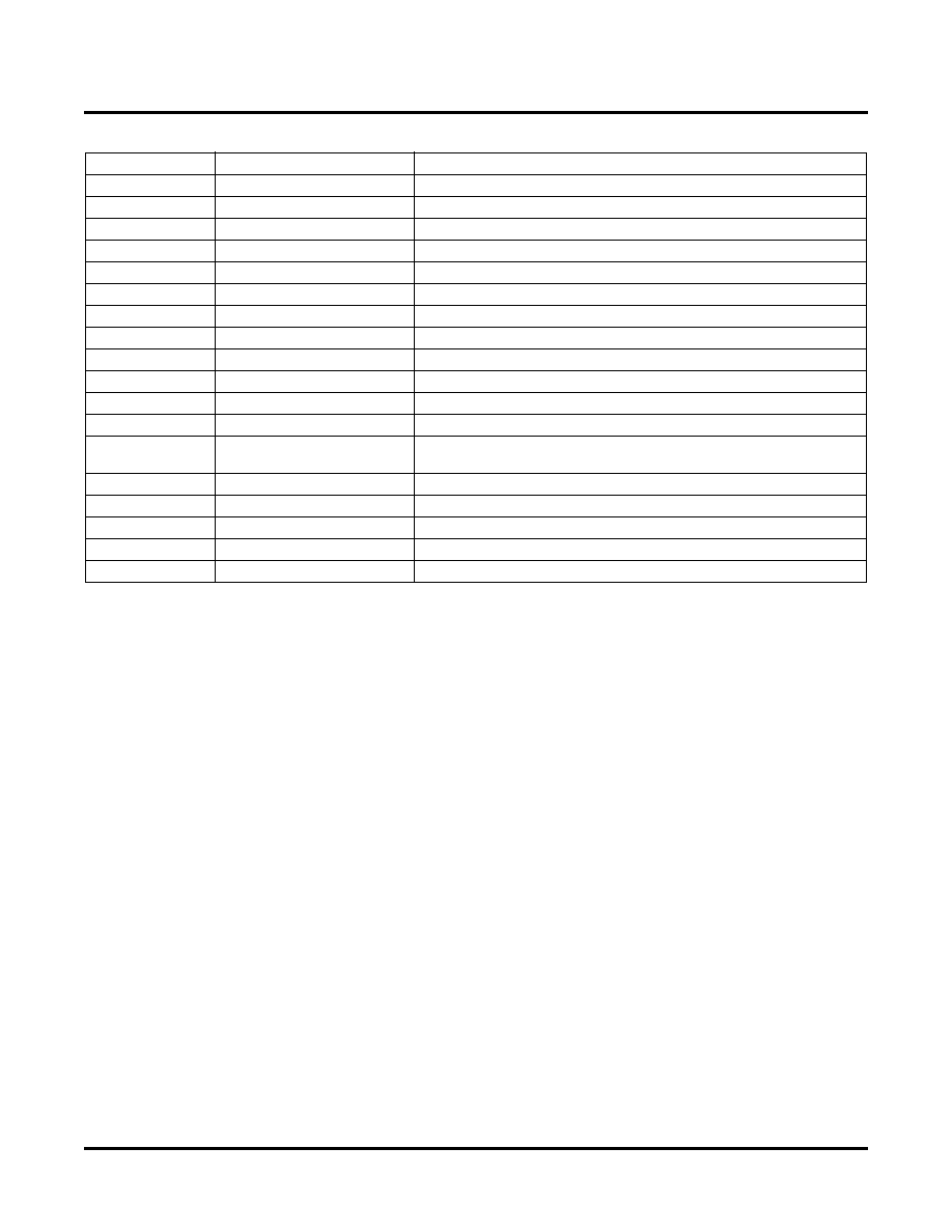
Table 2-12. PIO Signals List
PIO
The PIO contains four blocks: an input register block, output register block, tristate register block and a control logic
block. These blocks contain registers for operating in a variety of modes along with the necessary clock and selec-
tion logic.
Input Register Block
The input register blocks for PIOs in left, right and bottom edges contain delay elements and registers that can be
used to condition high-speed interface signals, such as DDR memory interfaces and source synchronous inter-
faces, before they are passed to the device core. Figure 2-29 shows the diagram of the input register block for left,
right and bottom edges. The input register block for the top edge contains one memory element to register the input
signal as shown in Figure 2-30. The following description applies to the input register block for PIOs in the left, right
and bottom edges of the device.
Input signals are fed from the sysI/O buffer to the input register block (as signal DI). If desired, the input signal can
bypass the register and delay elements and be used directly as a combinatorial signal (INDD), a clock (INCK) and,
in selected blocks, the input to the DQS delay block. If an input delay is desired, designers can select either a xed
delay or a dynamic delay DEL[3:0]. The delay, if selected, reduces input register hold time requirements when
using a global clock.
The input block allows three modes of operation. In the single data rate (SDR) the data is registered, by one of the
registers in the single data rate sync register block, with the system clock. In DDR Mode, two registers are used to
sample the data on the positive and negative edges of the DQS signal, creating two data streams, D0 and D1.
These two data streams are synchronized with the system clock before entering the core. Further discussion on
this topic is in the DDR Memory section of this data sheet.
Name
Type
Description
CE0, CE1
Control from the core
Clock enables for input and output block ip-ops
CLK0, CLK1
Control from the core
System clocks for input and output blocks
ECLK1, ECLK2
Control from the core
Fast edge clocks
LSR
Control from the core
Local Set/Reset
GSRN
Control from routing
Global Set/Reset (active low)
INCK
2
Input to the core
Input to Primary Clock Network or PLL reference inputs
DQS
Input to PIO
DQS signal from logic (routing) to PIO
INDD
Input to the core
Unregistered data input to core
INFF
Input to the core
Registered input on positive edge of the clock (CLK0)
IPOS0, IPOS1
Input to the core
Double data rate registered inputs to the core
QPOS0
1, QPOS11
Input to the core
Gearbox pipelined inputs to the core
QNEG0
1, QNEG11
Input to the core
Gearbox pipelined inputs to the core
OPOS0, ONEG0,
OPOS2, ONEG2
Output data from the core
Output signals from the core for SDR and DDR operation
OPOS1 ONEG1
Tristate control from the core
Signals to Tristate Register block for DDR operation
DEL[3:0]
Control from the core
Dynamic input delay control bits
TD
Tristate control from the core
Tristate signal from the core used in SDR operation
DDRCLKPOL
Control from clock polarity bus Controls the polarity of the clock (CLK0) that feed the DDR input block
DQSXFER
Control from core
Controls signal to the Output block
1. Signals available on left/right/bottom only.
2. Selected I/O.
相關(guān)PDF資料 |
PDF描述 |
|---|---|
| LFSCM3GA80EP1-6FCN1704C | |
| LFSC3GA15E-6FN256I | |
| LFSCM3GA40EP1-5FFN1020I | |
| LFXP2-40E-6FN484I | |
| LFXP2-17E-7F484C | |
相關(guān)代理商/技術(shù)參數(shù) |
參數(shù)描述 |
|---|---|
| LFE212SE-6FN256I | 制造商:LATTICE 制造商全稱:Lattice Semiconductor 功能描述:LatticeECP2/M Family Data Sheet |
| LFE2-12SE-6FN484C | 功能描述:FPGA - 現(xiàn)場可編程門陣列 12K LUTs S-Series 1.1.2V -6 Spd RoHS:否 制造商:Altera Corporation 系列:Cyclone V E 柵極數(shù)量: 邏輯塊數(shù)量:943 內(nèi)嵌式塊RAM - EBR:1956 kbit 輸入/輸出端數(shù)量:128 最大工作頻率:800 MHz 工作電源電壓:1.1 V 最大工作溫度:+ 70 C 安裝風(fēng)格:SMD/SMT 封裝 / 箱體:FBGA-256 |
| LFE212SE-6FN484C | 制造商:LATTICE 制造商全稱:Lattice Semiconductor 功能描述:LatticeECP2/M Family Data Sheet |
| LFE2-12SE-6FN484I | 功能描述:FPGA - 現(xiàn)場可編程門陣列 12K LUTs S-Ser 1.2V -6 Spd I RoHS:否 制造商:Altera Corporation 系列:Cyclone V E 柵極數(shù)量: 邏輯塊數(shù)量:943 內(nèi)嵌式塊RAM - EBR:1956 kbit 輸入/輸出端數(shù)量:128 最大工作頻率:800 MHz 工作電源電壓:1.1 V 最大工作溫度:+ 70 C 安裝風(fēng)格:SMD/SMT 封裝 / 箱體:FBGA-256 |
| LFE212SE-6FN484I | 制造商:LATTICE 制造商全稱:Lattice Semiconductor 功能描述:LatticeECP2/M Family Data Sheet |
發(fā)布緊急采購,3分鐘左右您將得到回復(fù)。