- 您現(xiàn)在的位置:買賣IC網(wǎng) > PDF目錄360707 > IBMN364164CT3C-68 x16 SDRAM PDF資料下載
參數(shù)資料
| 型號: | IBMN364164CT3C-68 |
| 英文描述: | x16 SDRAM |
| 中文描述: | x16內(nèi)存 |
| 文件頁數(shù): | 9/71頁 |
| 文件大?。?/td> | 1251K |
| 代理商: | IBMN364164CT3C-68 |
第1頁第2頁第3頁第4頁第5頁第6頁第7頁第8頁當(dāng)前第9頁第10頁第11頁第12頁第13頁第14頁第15頁第16頁第17頁第18頁第19頁第20頁第21頁第22頁第23頁第24頁第25頁第26頁第27頁第28頁第29頁第30頁第31頁第32頁第33頁第34頁第35頁第36頁第37頁第38頁第39頁第40頁第41頁第42頁第43頁第44頁第45頁第46頁第47頁第48頁第49頁第50頁第51頁第52頁第53頁第54頁第55頁第56頁第57頁第58頁第59頁第60頁第61頁第62頁第63頁第64頁第65頁第66頁第67頁第68頁第69頁第70頁第71頁
IBMN364164
IBMN364404
IBMN364804
64Mb Synchronous DRAM - Die Revision C
19L3265.E35856B
1/01
IBM Corporation. All rights reserved.
Use is further subject to the provisions at the end of this document.
Page 9 of 71
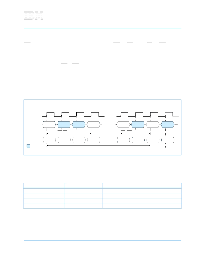
Bank Activate Command
In relation to the operation of a fast page mode DRAM, the Bank Activate command corresponds to a falling
RAS signal. The Bank Activate command is issued by holding CAS and WE high with CS and RAS low at the
rising edge of the clock. The bank select address A12 - A13 is used to select the desired bank. The row
address A0 - A11 is used to determine which row to activate in the selected bank.
The Bank Activate command must be applied before any Read or Write operation can be executed. The
delay from when the Bank Activate command is applied to when the first read or write operation can begin
must meet or exceed the RAS to CAS delay time (t
RCD
). Once a bank has been activated it must be pre-
charged before another Bank Activate command can be applied to the same bank. The minimum time inter-
val between successive Bank Activate commands to the same bank is determined by the RAS cycle time of
the device (t
RC
). The minimum time interval between interleaved Bank Activate commands (Bank A to Bank B
and vice versa) is the Bank to Bank delay time (t
RRD
). The maximum time that each bank can be held active
is specified as t
RAS(max)
.
Bank Select
The Bank Select inputs, BS0 and BS1, determine the bank to be used during a Bank Activate, Precharge,
Read, or Write operation.
Bank Activate Command Cycle
Bank Selection Bits
BS0
BS1
Bank
0
0
Bank 0
0
1
Bank 1
1
0
Bank 2
1
1
Bank 3
ADDRESS
CLK
T0
T2
T1
T3
Tn
Tn+1
Tn+2
Tn+3
COMMAND
NOP
NOP
NOP
NOP
Bank A
Row Addr.
Bank A
Activate
PWrite A
Bank A
Col. Addr.
. . . . . . . . . .
. . . . . . . . . .
. . . . . . . . . .
Bank B
Activate
Bank A
Row Addr.
Bank A
Activate
RAS-CAS delay (
t
RCD
)
: “H” or “L”
RAS Cycle time (
t
RC
)
RAS - RAS delay time (
t
RRD
)
Bank B
Row Addr.
(CAS Latency = 3, t
RCD
= 3)
相關(guān)PDF資料 |
PDF描述 |
|---|---|
| IBMN364164CT3C-75A | x16 SDRAM |
| IBMN364404CT3C-260 | x4 SDRAM |
| IBMN364404CT3C-360 | x4 SDRAM |
| IBMN364404CT3C-75A | x4 SDRAM |
| IBMN364804CT3C-260 | x8 SDRAM |
相關(guān)代理商/技術(shù)參數(shù) |
參數(shù)描述 |
|---|---|
| IBMPPC403GAJC33C1 | 制造商:IBM 功能描述: |
| IBMPPC750CLGEQ4023 | 制造商:IBM 功能描述:MPU 750CL RISC 32BIT 90NM 400MHZ 1.15V/1.8V 278FCBGA - Trays |
| IBMPPC750CLGEQ5023 | 制造商:IBM Microelectronics 功能描述:MPU 750CL RISC 32BIT 90NM 500MHZ 1.15V/1.8V 278FCBGA - Trays |
| IBMPPC750CLGEQA033 | 制造商:IBM 功能描述:MPU 750CL RISC 32BIT 90NM 1GHZ 1.15V/1.8V 278FCBGA - Trays 制造商:IBM 功能描述:IBMIBMPPC750CLGEQA033 CPU PPC 750CL 1GHZ |
| IBN100 | 制造商:Hubbell Wiring Device-Kellems 功能描述:ICON, BLANK,BR,100PK |
發(fā)布緊急采購,3分鐘左右您將得到回復(fù)。