- 您現在的位置:買賣IC網 > PDF目錄293971 > 5962R0722402VYC (ATMEL CORP) SPECIALTY MICROPROCESSOR CIRCUIT, PQFP256 PDF資料下載
參數資料
| 型號: | 5962R0722402VYC |
| 廠商: | ATMEL CORP |
| 元件分類: | 微控制器/微處理器 |
| 英文描述: | SPECIALTY MICROPROCESSOR CIRCUIT, PQFP256 |
| 封裝: | QFP-256 |
| 文件頁數: | 105/155頁 |
| 文件大小: | 4139K |
| 代理商: | 5962R0722402VYC |
第1頁第2頁第3頁第4頁第5頁第6頁第7頁第8頁第9頁第10頁第11頁第12頁第13頁第14頁第15頁第16頁第17頁第18頁第19頁第20頁第21頁第22頁第23頁第24頁第25頁第26頁第27頁第28頁第29頁第30頁第31頁第32頁第33頁第34頁第35頁第36頁第37頁第38頁第39頁第40頁第41頁第42頁第43頁第44頁第45頁第46頁第47頁第48頁第49頁第50頁第51頁第52頁第53頁第54頁第55頁第56頁第57頁第58頁第59頁第60頁第61頁第62頁第63頁第64頁第65頁第66頁第67頁第68頁第69頁第70頁第71頁第72頁第73頁第74頁第75頁第76頁第77頁第78頁第79頁第80頁第81頁第82頁第83頁第84頁第85頁第86頁第87頁第88頁第89頁第90頁第91頁第92頁第93頁第94頁第95頁第96頁第97頁第98頁第99頁第100頁第101頁第102頁第103頁第104頁當前第105頁第106頁第107頁第108頁第109頁第110頁第111頁第112頁第113頁第114頁第115頁第116頁第117頁第118頁第119頁第120頁第121頁第122頁第123頁第124頁第125頁第126頁第127頁第128頁第129頁第130頁第131頁第132頁第133頁第134頁第135頁第136頁第137頁第138頁第139頁第140頁第141頁第142頁第143頁第144頁第145頁第146頁第147頁第148頁第149頁第150頁第151頁第152頁第153頁第154頁第155頁
AT697F PRELIMINARY INFORMATION
53
7703D–AERO–12/09
PR
ELI
MINA
R
Y
IN
FOR
M
AT
IO
N
load/store instruction types. The PCI bus foresees 32 bit wide transactions with byte-enables for
each byte lane.
Initiator Mapping
For standard operation, the PCI interface only works in a limited address range. The address
range for such initiator transaction is limited to addresses between 0xA0000000 and
0xF0000000.
PCI addresses outside of this predefined range can be accessed only via DMA transactions.
Instructions of different width (byte, half-word, word, double) can be performed for each address
of the PCI address range. The three low significant bits of the address A[2:0] are used to deter-
mine which PCI byte enable line C/BE*[3:0] should be active during the transaction.
According to the SPARC architecture, big-endian mapping is implemented, the most significant
byte standing at the lower address (0x..00) and the least significant byte standing to the upper
address (0x..03).
A byte-writing to A[1:0] = 00 results in the byte enable pattern 0111, indicating that the e most
significant byte lane (bits 31:24) of the PCI data bus is selected.
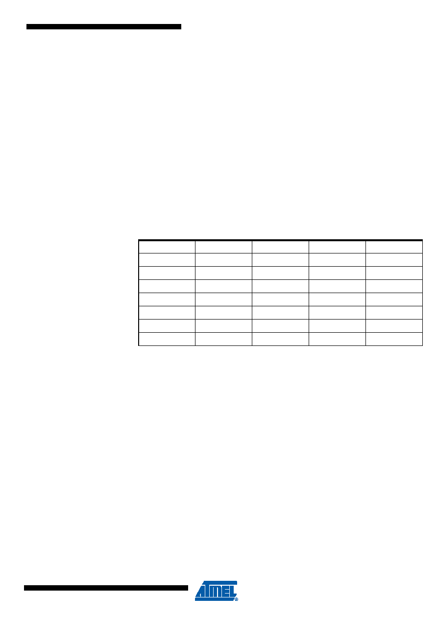
The following table presents the transaction width authorized for PCI transfers.
Table 20. Byte Enable Settings
width
8
16
32
64
Assembler
ld[s/u]b, stb
ld[s/u]h, sth
ld, st
ldd, std
C-datatype
char
short
int
long long
A[2:0]=000
0111
0011
0000
0000 (burst)
A[2:0]=100
0111
0011
0000
not aligned
A[2:0]=x01
1011
not aligned
A[2:0]=x10
1101
1100
not aligned
A[2:0]=x11
1110
not aligned
Note:
PCI byte enables are active low.
For non-aligned accesses, the byte enable pattern (1111) is issued on PCI, to avoid destroying
data in the remote PCI target.
Memory cycles
Many memory transactions such as memory-read/write and memory-read-line/write-invalidate
can be issued from the processor with common SPARC instruction set. Selection of the com-
mand to execute is performed setting the value PCIIC COMMSB.
Setting logical ‘01’ in PCIIC COMMSB result in the generation of memory read/write access
when PCI address is accessed. A logical value of ‘10’ result in a memory read line or write and
invalidate on PCI address access.
For the memory commands the address issued on the PCI bus is a word address with bits (1:0)
set to 00. This indicates that the linear incrementing mode is used.
operation
The following procedure shall be used to engage memory transaction on the PCI interface:
1.
Select the initiator mode by setting logical one in the PCIIC MOD.
2.
Select the memory load/store command or the memory read-line/write and invalidate
command in the PCI initiator configuration register. The PCIIC COMMSB shall be set
logical ‘01’ for simple load/store operation and shall be set logical ’11’ for read-line/write-
&-invalidate.
相關PDF資料 |
PDF描述 |
|---|---|
| 5962R8958702VXA | 5 V FIXED POSITIVE LDO REGULATOR, 1 V DROPOUT, CDSO16 |
| 5962R9215311VTA | 32K X 8 STANDARD SRAM, 55 ns, CDFP36 |
| 5962R9215311VTX | 32K X 8 STANDARD SRAM, 55 ns, CDFP36 |
| 5962G9215309VMX | 32K X 8 STANDARD SRAM, 55 ns, CDIP28 |
| 5962F9215315VMC | 32K X 8 STANDARD SRAM, 70 ns, CDIP28 |
相關代理商/技術參數 |
參數描述 |
|---|---|
| 5962R0722601VZA | 制造商:Texas Instruments 功能描述:D/A CONVERTER, 12-BIT - Trays |
| 5962R0722701VZA | 功能描述:模數轉換器 - ADC 8-Ch 50 kSPS-1 MSPS RoHS:否 制造商:Texas Instruments 通道數量:2 結構:Sigma-Delta 轉換速率:125 SPs to 8 KSPs 分辨率:24 bit 輸入類型:Differential 信噪比:107 dB 接口類型:SPI 工作電源電壓:1.7 V to 3.6 V, 2.7 V to 5.25 V 最大工作溫度:+ 85 C 安裝風格:SMD/SMT 封裝 / 箱體:VQFN-32 |
| 5962R0722902VXA | 功能描述:低壓差穩(wěn)壓器 - LDO 3-Terminal Adj Reg RoHS:否 制造商:Texas Instruments 最大輸入電壓:36 V 輸出電壓:1.4 V to 20.5 V 回動電壓(最大值):307 mV 輸出電流:1 A 負載調節(jié):0.3 % 輸出端數量: 輸出類型:Fixed 最大工作溫度:+ 125 C 安裝風格:SMD/SMT 封裝 / 箱體:VQFN-20 |
| 5962R0722961VXA | 功能描述:低壓差穩(wěn)壓器 - LDO 3-Terminal Adj Reg RoHS:否 制造商:Texas Instruments 最大輸入電壓:36 V 輸出電壓:1.4 V to 20.5 V 回動電壓(最大值):307 mV 輸出電流:1 A 負載調節(jié):0.3 % 輸出端數量: 輸出類型:Fixed 最大工作溫度:+ 125 C 安裝風格:SMD/SMT 封裝 / 箱體:VQFN-20 |
| 5962R0724902VPC | 制造商:Intersil Corporation 功能描述: |
發(fā)布緊急采購,3分鐘左右您將得到回復。