- 您現(xiàn)在的位置:買賣IC網(wǎng) > PDF目錄383982 > UPD703204 (NEC Corp.) 32-BIT SINGLE-CHIP MICROCONTROLLERS PDF資料下載
參數(shù)資料
| 型號: | UPD703204 |
| 廠商: | NEC Corp. |
| 英文描述: | 32-BIT SINGLE-CHIP MICROCONTROLLERS |
| 中文描述: | 32位單晶片微控制器 |
| 文件頁數(shù): | 15/98頁 |
| 文件大小: | 797K |
| 代理商: | UPD703204 |
第1頁第2頁第3頁第4頁第5頁第6頁第7頁第8頁第9頁第10頁第11頁第12頁第13頁第14頁當(dāng)前第15頁第16頁第17頁第18頁第19頁第20頁第21頁第22頁第23頁第24頁第25頁第26頁第27頁第28頁第29頁第30頁第31頁第32頁第33頁第34頁第35頁第36頁第37頁第38頁第39頁第40頁第41頁第42頁第43頁第44頁第45頁第46頁第47頁第48頁第49頁第50頁第51頁第52頁第53頁第54頁第55頁第56頁第57頁第58頁第59頁第60頁第61頁第62頁第63頁第64頁第65頁第66頁第67頁第68頁第69頁第70頁第71頁第72頁第73頁第74頁第75頁第76頁第77頁第78頁第79頁第80頁第81頁第82頁第83頁第84頁第85頁第86頁第87頁第88頁第89頁第90頁第91頁第92頁第93頁第94頁第95頁第96頁第97頁第98頁
Preliminary Product Information U15436EJ1V0PM
15
μ
PD703201, 703201Y, 703204, 703204Y, 70F3201, 70F3201Y, 70F3204, 70F3204Y
(2/4)
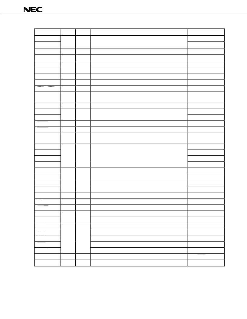
Pin Name
I/O
PULL
Function
Alternate Function
ANO0
P80
ANO1
Output
No
Analog voltage output for D/A converter
P81
ASTB
Output
No
Address strobe signal output for external memory
PCT6
AV
DD
–
–
Positive power supply for A/D converter (same potential as V
DD
)
–
AV
REF0
Reference voltage input for A/D converter
–
AV
REF1
Input
–
Reference voltage input for D/A converter
–
AV
SS
–
–
Ground potential for A/D, D/A converters (same potential as V
SS
)
–
CLKOUT
Output
No
Internal system clock output
PCM1
CS0 to CS3
Output
No
Chip select output
PCS0 to PCS3
EV
DD
–
–
Positive power supply for external devices (same potential as
V
DD
)
–
EV
SS
–
–
Ground potential for external devices (same potential as V
SS
)
–
FLMD0
Note 1
–
FLMD1
Note 1
Input
No
Flash programming mode lead-in pins
PDL5/AD5
HLDAK
Output
No
Bus hold acknowledge output
PCM2
HLDRQ
Input
No
Bus hold request input
PCM3
IC
–
–
Internally connected (directly connect to V
SS
). (
μ
PD703201,
703201Y, 703204, and 703204Y only)
–
INTP0 to INTP3
P01/TI2 to P04/TI5
INTP4
P05
INTP5
P92/A2
INTP6
Input
Yes
External interrupt request input (maskable, analog noise
elimination)
P93/A3
INTP00
P43/TI0/TCLR0
INTP01
Capture trigger input (TM0)
P44/TO0
INTP10
P45/TI1/TCLR1
INTP11
Input
Yes
Capture trigger input (TM1)
P46/TO1
NMI
Input
Yes
External interrupt input (non-maskable, analog noise elimination)
P00
RD
Output
No
Read strobe signal output for external memory
PCT4
RESET
Input
–
System reset input
–
RXD0
Serial receive data input (UART0)
P30/SI1
RXD1
Input
Yes
Serial receive data input (UART1)
P98/A8
SCK0
Serial clock I/O (CSI0)
P42/SCL
Note 2
SCK1
Serial clock I/O (CSI1)
P32
SCK2
Serial clock I/O (CSI2)
P912/A12
SCK3
Serial clock I/O (CSI3)
P915/A15
[SCK4]
I/O
Yes
Serial clock I/O (CSI4)
[P22]
SCL
Note 2
I/O
Yes
Serial clock I/O (I
2
C)
P42/SCK0
SDA
Note 2
I/O
Yes
Serial transmit/receive data I/O (I
2
C)
P41/SO0
Notes 1.
Applies to the
μ
PD70F3201, 70F3201Y, 70F3204, and 70F3204Y only.
2.
Applies to the
μ
PD703201Y, 703204Y, 70F3201Y, and 70F3204Y only.
Remarks 1.
PULL: On-chip pull-up resistor
2.
Pins in brackets ([ ]) are only for the V850ES/SA3.
相關(guān)PDF資料 |
PDF描述 |
|---|---|
| UPD70F30025AGC-25 | LJT 24C 12#16 12#12 PIN PLUG |
| UPD70F3004AGC-33 | 32-bit RISC Microcontrollers |
| UPD70F3004AGC-25 | 32-bit RISC Microcontrollers |
| UPD7030025AGC-25 | LJT 24C 12#16 12#12 PIN PLUG |
| UPD70F30025AGC-33 | LJT 29C 29#16 PIN PLUG |
相關(guān)代理商/技術(shù)參數(shù) |
參數(shù)描述 |
|---|---|
| UPD703204F1-XXX-EA6 | 制造商:NEC 制造商全稱:NEC 功能描述:32-BIT SINGLE-CHIP MICROCONTROLLERS |
| UPD703204Y | 制造商:NEC 制造商全稱:NEC 功能描述:32-BIT SINGLE-CHIP MICROCONTROLLERS |
| UPD703204YF1-XXX-EA6 | 制造商:NEC 制造商全稱:NEC 功能描述:32-BIT SINGLE-CHIP MICROCONTROLLERS |
| UPD703208 | 制造商:NEC 制造商全稱:NEC 功能描述:32-Bit Single-Chip Microcontrollers |
| UPD703208A | 制造商:NEC 制造商全稱:NEC 功能描述:32-Bit Single-Chip Microcontrollers |
發(fā)布緊急采購,3分鐘左右您將得到回復(fù)。