- 您現(xiàn)在的位置:買賣IC網(wǎng) > PDF目錄384010 > TLV5592 (Texas Instruments, Inc.) 2-BIT ANALOG-TO-DIGITAL CONVERTER FOR FLEX PAGER CHIPSET PDF資料下載
參數(shù)資料
| 型號(hào): | TLV5592 |
| 廠商: | Texas Instruments, Inc. |
| 英文描述: | 2-BIT ANALOG-TO-DIGITAL CONVERTER FOR FLEX PAGER CHIPSET |
| 中文描述: | 2位模擬數(shù)字轉(zhuǎn)換器對(duì)于Flex尋呼機(jī)芯片組 |
| 文件頁(yè)數(shù): | 4/15頁(yè) |
| 文件大小: | 208K |
| 代理商: | TLV5592 |
第1頁(yè)第2頁(yè)第3頁(yè)當(dāng)前第4頁(yè)第5頁(yè)第6頁(yè)第7頁(yè)第8頁(yè)第9頁(yè)第10頁(yè)第11頁(yè)第12頁(yè)第13頁(yè)第14頁(yè)第15頁(yè)
TLV5592
2-BIT ANALOG-TO-DIGITAL CONVERTER
FOR FLEX PAGER CHIPSET
SLAS145A – JUNE1996 – REVISED DECEMBER 1997
4
POST OFFICE BOX 655303
DALLAS, TEXAS 75265
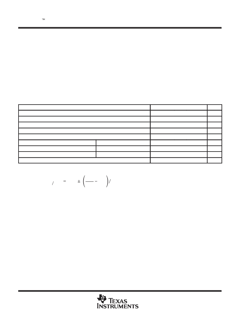
absolute maximum ratings over operating free-air temperature range (unless otherwise noted)
Supply voltage range, AV
DD
, DV
DD
Input voltage range, V
I
Output voltage range, EXTS0, EXTS1
Offset input voltage, V
IO
Peak input current (any input)
Operating free-air temperature range, T
A
Storage temperature range, T
stg
Lead temperature 1,6 mm (1/16 inch) from case for 10 seconds
–0.5 V to 6.5 V
. . . . . . . . . . . . . . . . . . . . . . . . . . . . . . . . . . . . . . . . . . . . . . . . .
. . . . . . . . . . . . . . . . . . . . . . . . . . . . . . . . . . . . . . . . . . . . . . . . . . . . .
. . . . . . . . . . . . . . . . . . . . . . . . . . . . . . . . . . . . . . .
. . . . . . . . . . . . . . . . . . . . . . . . . . . . . . . . . . . . . . . . . . . . . . . . . . .
. . . . . . . . . . . . . . . . . . . . . . . . . . . . . . . . . . . . . . . . . . . . . . . . . . . . . . . . . . . .
. . . . . . . . . . . . . . . . . . . . . . . . . . . . . . . . . . . . . . . . . . . .
. . . . . . . . . . . . . . . . . . . . . . . . . . . . . . . . . . . . . . . . . . . . . . . . . . .
–0.3 V to AV
DD
+ 0.3 V
–0.3 V to DV
DD
+ 0.3 V
–0.3 V to AV
DD
+ 0.3 V
±
20 mA
–20
°
C to 65
°
C
–65
°
C to 150
°
C
260
°
C
. . . . . . . . . . . . . . . . . . . . . . . . . . . . . . .
Stresses beyond those listed under “absolute maximum ratings” may cause permanent damage to the device. These are stress ratings only, and
functional operation of the device at these or any other conditions beyond those indicated under “recommended operating conditions” is not
implied. Exposure to absolute-maximum-rated conditions for extended periods may affect device reliability.
recommended operating conditions
MIN
NOM
MAX
UNIT
Supply voltage, AVDD, DVDD
Power supply ripple
1.8
2.5
V
0.001
Vpp
kHz
Input clock frequency, f(CLK)
Input clock duty cycle
38.4
45
50
55
%
Voltage offset applied at DC OFFSET, VI(DC OFFSET) (see Note 2)
Analog input voltage, VI(pp) (See Note 1 )
High-level control input voltage, VIH
Low-level control input voltage, VIL
Operating free-air temperature, TA
0.25
VDD–0.25
VIO+0.355
0.2 DVDD
V
VDD = 2.0 V
VDD = 1.8 V to 2.4 V
VDD = 1.8 V to 2.4 V
VIO–0.355
Vpp
V
0.8 DVDD
–25
V
65
°
C
NOTES:
1. The TLV5592 functions and operates down to 1.8 V. Full electrical specifications are ensured from 1.8 to 2.5 V, unless otherwise
noted.
VDD
2
2.
V
I(MAX MIN)
V
IO
0.25
(
FILTER MAX GAIN)
This equation is valid for input sinusoids of less than 800 Hz.
相關(guān)PDF資料 |
PDF描述 |
|---|---|
| TLV5592D | 2-BIT ANALOG-TO-DIGITAL CONVERTER FOR FLEX PAGER CHIPSET |
| TLV5604D | 2.7-V TO 5.5-V 10-BIT 3-mS QUADRUPLE DIGITAL-TO-ANALOG CONVERTERS WITH POWER DOWN |
| TLV5604PW | 2.7-V TO 5.5-V 10-BIT 3-mS QUADRUPLE DIGITAL-TO-ANALOG CONVERTERS WITH POWER DOWN |
| TLV5606D | 2.7 V TO 5.5 V LOW POWER 10-BIT DIGITAL-TO-ANALOG CONVERTERS WITH POWER DOWN |
| TLV5606DGK | 2.7 V TO 5.5 V LOW POWER 10-BIT DIGITAL-TO-ANALOG CONVERTERS WITH POWER DOWN |
相關(guān)代理商/技術(shù)參數(shù) |
參數(shù)描述 |
|---|---|
| TLV5592D | 制造商:TI 制造商全稱:Texas Instruments 功能描述:2-BIT ANALOG-TO-DIGITAL CONVERTER FOR FLEX PAGER CHIPSET |
| TLV5592ED | 制造商:Texas Instruments 功能描述: |
| TLV5592EDR | 制造商:Texas Instruments 功能描述: |
| TLV5592EPWR | 制造商:Texas Instruments 功能描述:1.8 VOLT 2-BIT FLOATING ADC FOR FLEX PAGER CHIPSET - Tape and Reel |
| TLV5593VF | 制造商:Rochester Electronics LLC 功能描述:- Bulk 制造商:Texas Instruments 功能描述:5593VF |
發(fā)布緊急采購(gòu),3分鐘左右您將得到回復(fù)。