- 您現(xiàn)在的位置:買賣IC網(wǎng) > PDF目錄383804 > SCANPSC100FSC (FAIRCHILD SEMICONDUCTOR CORP) Embedded Boundary Scan Controller (IEEE 1149.1 Support) PDF資料下載
參數(shù)資料
| 型號(hào): | SCANPSC100FSC |
| 廠商: | FAIRCHILD SEMICONDUCTOR CORP |
| 元件分類: | 微控制器/微處理器 |
| 英文描述: | Embedded Boundary Scan Controller (IEEE 1149.1 Support) |
| 中文描述: | SPECIALTY MICROPROCESSOR CIRCUIT, PDSO28 |
| 封裝: | 0.300 INCH, MS-013, SOIC-28 |
| 文件頁(yè)數(shù): | 16/21頁(yè) |
| 文件大?。?/td> | 208K |
| 代理商: | SCANPSC100FSC |
第1頁(yè)第2頁(yè)第3頁(yè)第4頁(yè)第5頁(yè)第6頁(yè)第7頁(yè)第8頁(yè)第9頁(yè)第10頁(yè)第11頁(yè)第12頁(yè)第13頁(yè)第14頁(yè)第15頁(yè)當(dāng)前第16頁(yè)第17頁(yè)第18頁(yè)第19頁(yè)第20頁(yè)第21頁(yè)
www.fairchildsemi.com
16
S
Application Note
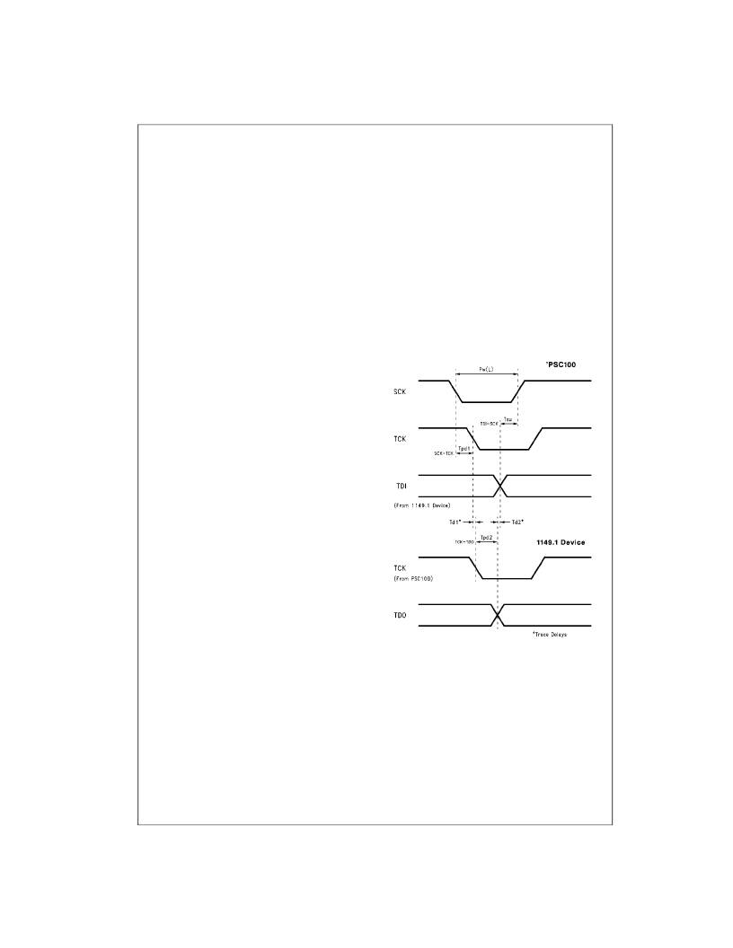
SCK MINIMUM PULSE WIDTH CALCULATION
The SCANPSC100 Parallel to Serial Converter is intended
to act as the interface between a processor and an IEEE
1149.1 boundary scan chain. When used in this configura-
tion, there is a critical timing situation that is not obvious.
This timing involves the system clock rate at which data
from the scan ring is being read into the SCANPSC100
’
s
TDI pin (target TAP controllers in SHIFT-DR or SHIFT-IR
states).
To fully understand the events which are taking place dur-
ing this critical period, it is useful to view the waveforms of
interest as they relate in time. See Figure 16. The TCK is
derived internally to the SCANPSC100 based on the sys-
tem clock (SCK) and clock gating control. The result is that
when TCK is running, it is at the same frequency as SCK
but delayed in time by the SCK-TCK propagation delay.
The TCK signal from the SCANPSC100 drives all of the
IEEE 1149.1 target devices. On the rising edge of TCK,
data present at each scan cell is clocked into it. On the fall-
ing edge, this data is presented at the output of the same
scan cell for the next adjacent cell to read. With regards to
the last cell in a particular target, the falling edge of TCK
presents the data in the last scan cell to the TDO pin, a
TCK-TDO propagation delay later.
At the SCANPSC100, data shifted in through the TDI pin is
clocked in on the rising edge of SCK, not TCK. The reason
for this is that TCK is generated internal to the
SCANPSC100 and intended to control the boundary scan
targets. The SCANPSC100 is controlled by SCK, therefore
the signal to be shifted into the TDI pin needs to be refer-
enced to SCK not TCK. New TDI data must be present a
TDI-SCK set-up time prior to the rising edge of SCK in
order to guarantee validity. Although SCK is usually contin-
uous, the TDI buffer is controlled by a SHIFT-ENABLE sig-
nal which is generated internal to the SCANPSC100,
based on the status of the TDI buffer and the Mode Regis-
ters.
We now see the three major timing components which limit
the duration of the SCK pulse width low. There are two
minor additional delays which should be noted. The TCK
signal from the SCANPSC100 needs to arrive at the target
device to be recognized, and this takes a finite amount of
time depending on the signal trace length and impedance.
Similarly, the TDO signal of the last target in the chain
needs to reach the TDI pin of the SCANPSC100, taking a
finite amount of time as well. These two trace delays can
be minimized by making the target device closest to the
SCANPSC100 the last device in the chain. See Figure 17.
PROGRAMMING RESTRICTIONS
Because certain mode bits enable shift operations for cer-
tain functions, these mode bits should not be changed
when shift operations are in progress. The alignment of all
registers during shift operations is controlled by a three bit
counter in the TCK control block. Enabling or disabling a
function in the middle of a shift operation may disrupt the
logic necessary to keep all shifter/buffers byte-aligned. For
example, if the TDO shifter/buffer (already loaded) is
enabled while the three bit counter value is three, the
shifter/buffer will only shift out 5 bits of the first byte loaded.
The following bits should not be changed when shift opera-
tions are in progress, i.e., when TCK is enabled (see TCK
control section):
MODE0(7:3)
MODE1(4:3)
MODE2(0)
Pw(L) minimum
=
t
PD1
+
t
D1
+
t
PD2
+
t
D2
+
t
SU
FIGURE 16. System Clock Timing
for Accurate TDI Data
相關(guān)PDF資料 |
PDF描述 |
|---|---|
| SCANPSC110FSC | SCAN Bridge Hierarchical and Multidrop Addressable JTAG Port (IEEE1149.1 System Test Support) |
| SCP-5453 | SOCKET,IC,16PIN,MACHINE TOOLED WIRE WRAP,0.3"WIDE,0.515"LEAD |
| SCP-6122 | POWER OPERATIONAL AMPLIFIER |
| SCS152 | HM Series Hermetically Sealed Basic Switch, Single Pole Double Throw Circuitry, 0.5 A at 28 Vdc, Integral Lever Actuator, Solder Termination |
| SCS152-IS | Small glass bead with axial leads |
相關(guān)代理商/技術(shù)參數(shù) |
參數(shù)描述 |
|---|---|
| SCANPSC100FSCX | 功能描述:接口 - 專用 Emb Boun Scan Cont RoHS:否 制造商:Texas Instruments 產(chǎn)品類型:1080p60 Image Sensor Receiver 工作電源電壓:1.8 V 電源電流:89 mA 最大功率耗散: 最大工作溫度:+ 85 C 安裝風(fēng)格:SMD/SMT 封裝 / 箱體:BGA-59 |
| SCANPSC110 | 制造商:NSC 制造商全稱:National Semiconductor 功能描述:SCAN Bridge Hierarchical and Multidrop Addressable JTAG Port (IEEE1149.1 System Test Support) |
| SCANPSC110_ZFC3026B WAF | 制造商:Fairchild Semiconductor Corporation 功能描述: |
| SCANPSC110F | 制造商:NSC 制造商全稱:National Semiconductor 功能描述:SCAN Bridge Hierarchical and Multidrop Addressable JTAG Port (IEEE1149.1 System Test Support) |
| SCANPSC110FDMQB | 制造商:NSC 制造商全稱:National Semiconductor 功能描述:SCAN Bridge Hierarchical and Multidrop Addressable JTAG Port (IEEE1149.1 System Test Support) |
發(fā)布緊急采購(gòu),3分鐘左右您將得到回復(fù)。