- 您現(xiàn)在的位置:買賣IC網(wǎng) > PDF目錄383804 > SCANPSC100FSC (FAIRCHILD SEMICONDUCTOR CORP) Embedded Boundary Scan Controller (IEEE 1149.1 Support) PDF資料下載
參數(shù)資料
| 型號: | SCANPSC100FSC |
| 廠商: | FAIRCHILD SEMICONDUCTOR CORP |
| 元件分類: | 微控制器/微處理器 |
| 英文描述: | Embedded Boundary Scan Controller (IEEE 1149.1 Support) |
| 中文描述: | SPECIALTY MICROPROCESSOR CIRCUIT, PDSO28 |
| 封裝: | 0.300 INCH, MS-013, SOIC-28 |
| 文件頁數(shù): | 10/21頁 |
| 文件大小: | 208K |
| 代理商: | SCANPSC100FSC |
www.fairchildsemi.com
10
S
Serial Scan Interface (SSI)
TCK CONTROL
TCK CONTROL is the central control block that enables or
disables shift operations and provides byte alignment for
the shifter/buffers. The state of all shifter/buffers and the
32-bit counter (CNT32) is evaluated here and TCK is
stopped and started. A clock enable circuit allows the
“
TCK
enable
”
signal to change only when SCK is LOW; there-
fore, TCK always stops LOW. TCK does not toggle
(remains LOW) under the following conditions:
TDO Shifter/Buffer is enabled and empty.
TDO Shifter/Buffer is enabled in PRPG mode and is not
fully loaded.
TDI Shifter/Buffer is enabled and full.
TDI Shifter/Buffer is enabled in SSC mode but is not fully
loaded with an initial value.
TMS0 Shifter/Buffer is enabled and empty.
TMS1 Shifter/Buffer is enabled and empty.
CNT32 is enabled but not loaded.
CNT32 is enabled and has reached terminal count.
Also included within the TCK control block in CNT3, a 3-bit
count up counter. CNT3 is included to maintain byte align-
ment within the shifter/buffers by providing a signal to tog-
gle between the two 8-bit FIFOs which comprise the shifter/
buffer. The toggling operation occurs, in an enabled shifter/
buffer, each time CNT3 counts 8 TCK cycles or when
CNT32 reaches terminal count. The CNT3 is reset to 0
when CNT32 reaches terminal count or after a PSC100
reset condition.
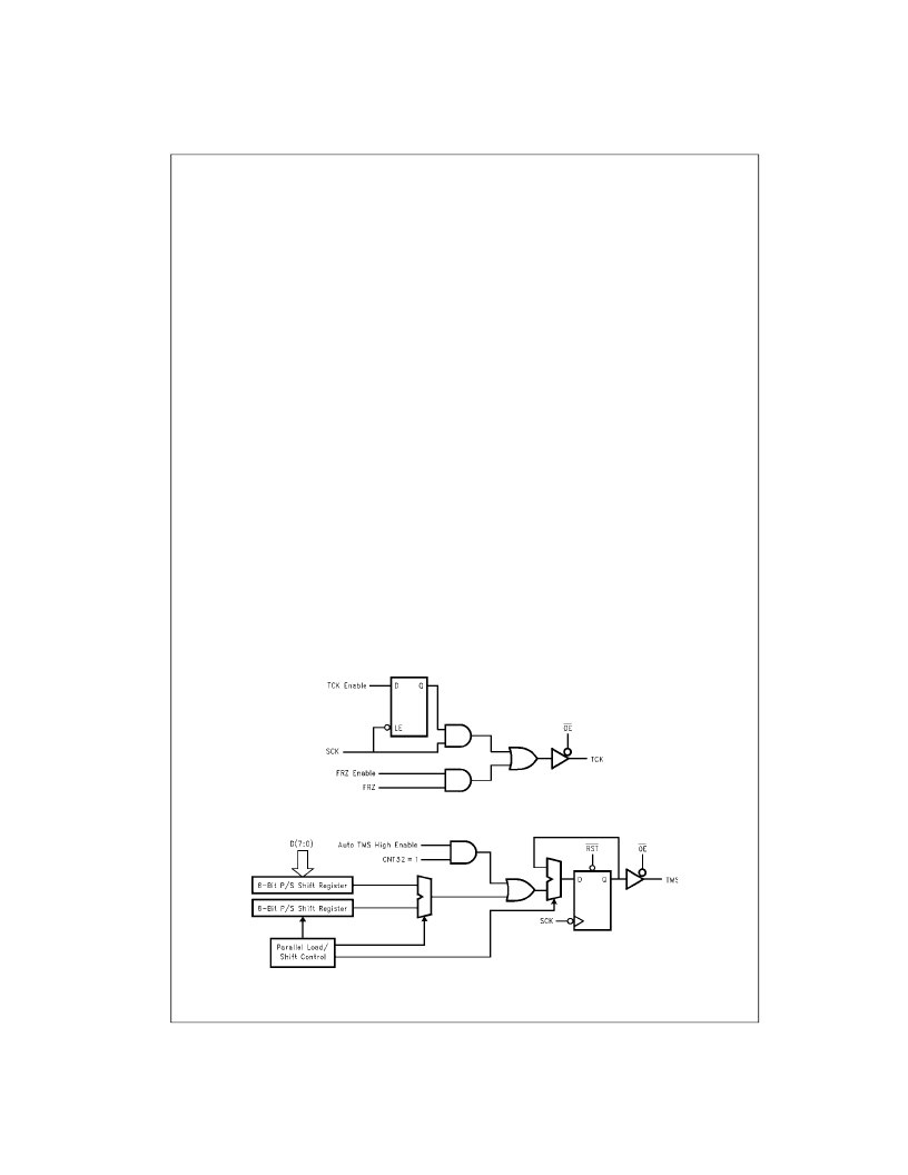
FREEZE MODE.
This mode is included in the TCK control
block to support the 1149.1 SAMPLE operation. The intent
of the SAMPLE instruction is to allow device input and out-
put levels to be observed during normal system operation.
Data is latched (or
“
sampled
”
) into the boundary scan reg-
isters when the TAP controller (see Figure 8 on previous
page) transitions from the Capture-DR state to the Shift-DR
state (if SAMPLE/ PRELOAD is the active instruction).
Synchronizing this
“
transition
”
(rising edge of TCK with
TMS at logic low) with a known system state is imperative
to an accurate pass/fail assessment. The Freeze Mode
provides a means of asynchronously creating the TCK
pulse via an external PSC100 pin. When the Freeze Pin
Enable bit (bit 2 in Mode Register 1) is set, a logic high on
the PSC100 FRZ input pin will cause TCK to go HIGH.
Once the transition is complete, the Freeze Mode can be
removed (i.e. Freeze Pin Enable bit returned to logic 0 or
Freeze pin forced LOW) and the sampled data can be
shifted out/evaluated using the
“
standard
”
PSC100 proto-
col. Figure 9 illustrates the logic implementation of the
Freeze feature. It should be noted that Freeze mode is sim-
ply gated with the TCK output and does not disable shift
operations within the shifter/buffers or disable CNT32.
Therefore, no shifting or TCK counting using CNT32
should be performed when Freeze mode is enabled.
The
“
standard
”
mode of TCK control uses CNT32 in con-
junction with the status registers to start and stop TCK. For
this mode, CNT32 is enabled and loaded with the number
of TCK cycles required to shift the desired bits to/from the
scan chain. The shifter/buffer(s) participating in the shift
operation is enabled and provides the necessary full/empty
status to stop TCK for processor writes/reads. This mode
of TCK control provides a systematic protocol for managing
PSC100 operations (specifically, handling partial bytes).
Another option for TCK control relies solely on the status of
the shifter/buffers (i.e., CNT32 is disabled) to start and stop
TCK. This option eliminates the time required to load
CNT32, but makes management of partial bytes (see
shifter/buffer description section) more cumbersome.
FIGURE 9. TCK Logic
FIGURE 10. TMS Shifter/Buffer Block Diagram
相關(guān)PDF資料 |
PDF描述 |
|---|---|
| SCANPSC110FSC | SCAN Bridge Hierarchical and Multidrop Addressable JTAG Port (IEEE1149.1 System Test Support) |
| SCP-5453 | SOCKET,IC,16PIN,MACHINE TOOLED WIRE WRAP,0.3"WIDE,0.515"LEAD |
| SCP-6122 | POWER OPERATIONAL AMPLIFIER |
| SCS152 | HM Series Hermetically Sealed Basic Switch, Single Pole Double Throw Circuitry, 0.5 A at 28 Vdc, Integral Lever Actuator, Solder Termination |
| SCS152-IS | Small glass bead with axial leads |
相關(guān)代理商/技術(shù)參數(shù) |
參數(shù)描述 |
|---|---|
| SCANPSC100FSCX | 功能描述:接口 - 專用 Emb Boun Scan Cont RoHS:否 制造商:Texas Instruments 產(chǎn)品類型:1080p60 Image Sensor Receiver 工作電源電壓:1.8 V 電源電流:89 mA 最大功率耗散: 最大工作溫度:+ 85 C 安裝風(fēng)格:SMD/SMT 封裝 / 箱體:BGA-59 |
| SCANPSC110 | 制造商:NSC 制造商全稱:National Semiconductor 功能描述:SCAN Bridge Hierarchical and Multidrop Addressable JTAG Port (IEEE1149.1 System Test Support) |
| SCANPSC110_ZFC3026B WAF | 制造商:Fairchild Semiconductor Corporation 功能描述: |
| SCANPSC110F | 制造商:NSC 制造商全稱:National Semiconductor 功能描述:SCAN Bridge Hierarchical and Multidrop Addressable JTAG Port (IEEE1149.1 System Test Support) |
| SCANPSC110FDMQB | 制造商:NSC 制造商全稱:National Semiconductor 功能描述:SCAN Bridge Hierarchical and Multidrop Addressable JTAG Port (IEEE1149.1 System Test Support) |
發(fā)布緊急采購,3分鐘左右您將得到回復(fù)。