- 您現(xiàn)在的位置:買賣IC網(wǎng) > PDF目錄383804 > SA2400A (NXP Semiconductors N.V.) Single chip transceiver for 2.45 GHz ISM band PDF資料下載
參數(shù)資料
| 型號: | SA2400A |
| 廠商: | NXP Semiconductors N.V. |
| 英文描述: | Single chip transceiver for 2.45 GHz ISM band |
| 中文描述: | 單為2.45 GHz的ISM頻帶收發(fā)器芯片 |
| 文件頁數(shù): | 22/34頁 |
| 文件大小: | 325K |
| 代理商: | SA2400A |
第1頁第2頁第3頁第4頁第5頁第6頁第7頁第8頁第9頁第10頁第11頁第12頁第13頁第14頁第15頁第16頁第17頁第18頁第19頁第20頁第21頁當前第22頁第23頁第24頁第25頁第26頁第27頁第28頁第29頁第30頁第31頁第32頁第33頁第34頁
Philips Semiconductors
Product data
SA2400A
Single chip transceiver for 2.45 GHz ISM band
2002 Nov 04
22
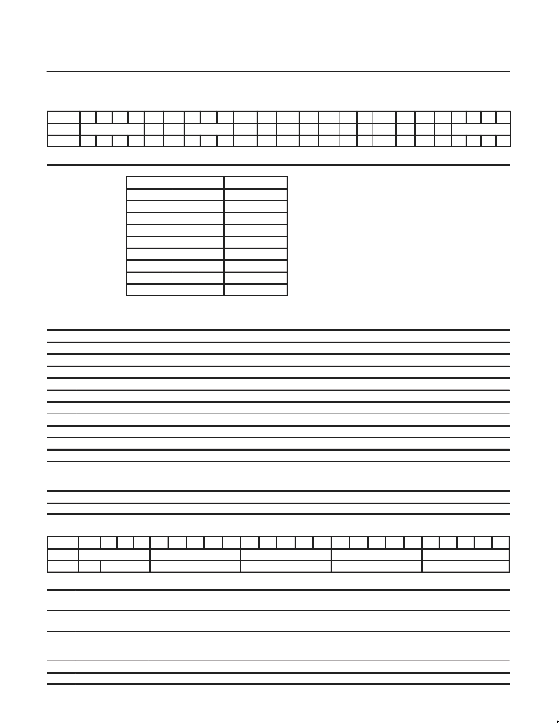
Table 18. Address 04:
Main chip operation modes, filter tuner, other controls
Bit
Name
Default
23
22
‘0000’
0
21
20
19
adc
0
18
fterr
0
17
16
15
14
v2p5
0
13
I1m
0
12
I0p3
1
11
n.u.
0
10
in22
0
9
8
xo
1
7
6
5
4
3
2
1
0
Filttune
1
clk
1
digin
0
rxlv
0
veo
0
vei
0
Chip mode
0
0
0
0
0
1
0
0
0
Bit #
0–3
Name
Chip mode
Description
Main mode of operation. Coding according to following table:
Bit3
Bit2
Bit1
Bit0
Mode
0
0
0
0
SLEEP
0
0
0
1
TX/RX
0
0
1
0
WAIT
0
0
1
1
RXMGC
0
1
0
0
FCALIB
0
1
0
1
DCALIB
0
1
1
0
FASTTXRXMGC
0
1
1
1
RESET
1
0
0
0
VCOCALIB
Notes on modes:
All calibration modes (*CALIB) require the crystal oscillator to be ON (bit XO = 1).
DCALIB (Tx LO leakage calibration) requires being in Tx mode for 5
μ
s before calibration.
Use external vco input (vcoextin)
Make internal vco available at vco pads (vcoextout)
Rx output common mode voltage: 0–V
DD
/2, 1–1.25 V
Use digital Tx inputs (FIRDAC)
Xtal oscillator ON
Reference clock output ON
Xtal input frequency: 0–44 MHz, 1–22 MHz
4
5
6
7
8
9
10
11
12
13
14
15–17
vei
veo
rxlv
digin
xo
clk
in22
Not used
I0p3
I1m
v2p5
filttune
External reference current (pad idcout): 0.3 mA to ground
External reference current (pad idcout): 1.0 mA from supply
External reference voltage (pad v2p5) ON
Rx and Tx filter tuning bits:
Write:
(with test mode only), these bits set tuning value
Read:
(in normal mode) tuner setting can be read out here
18
19
fterr
adc
Filter tuner error (read only): result is 1 when tuner exceeded range
‘1’: in Rx mode, the RSSI-ADC is always on.
‘0’: the RSSI-ADC is only on during AGC operation.
Table 19. Address 05:
AGC adjustment settings
Bit
Name
Default
23
22
21
20
19
18
Rx AGC Gmax
79 dB – 11001
17
16
15
14
13
12
11
10
9
8
7
6
5
4
AGC_rxondel/sample1
27(4.9
μ
s) – 11011
3
2
1
0
Rx AGC target
±
(0)
AGC_bbdel/ADCval
7(1.3
μ
s) – 00111
AGC_lnadel/sample2
15(2.7
μ
s) – 01111
val(000)
Bit #
0–4
Name
AGC_rxondel/s1
Description
Write:
Programmable delay for AGC algorithm: Rx turn-on to AGCSET. In units of 182 ns (5.5 MHz)
Read:
1
st
sample of RSSI in AGC cycle
Write:
Programmable delay for AGC algorithm: Settling time after LNA gain switching. In units of 182 ns (5.5 MHz)
Read:
2
nd
sample of RSSI in AGC cycle
Write:
Programmable delay for AGC algorithm: Settling time after baseband gain switching. In units of 182 ns
(5.5 MHz)
Read:
Output of RSSI/Tx–peak detector ADC in 5-bit Gray code
5–9
AGC_lnadel/s2
10–14
AGC_bbdel/ADCval
15–19
20–23
AGC Gmax
AGC target
Rx AGC gain limit (54 dB + programmed value) (valid: 54 through 85)
Adjustment value to AGC settling target, range –7 dB
…
7 dB (sign plus three bits)
相關PDF資料 |
PDF描述 |
|---|---|
| SA2400ABE | Single chip transceiver for 2.45 GHz ISM band |
| SA5522 | 1.4 GHz I2C-bus controlled synthesizer |
| SA572F | Programmable analog compandor |
| SAA2013HB-S | Digital Audio Tape Circuit |
| SAA2500GP | Video Processing/ENDEC for MPEG |
相關代理商/技術參數(shù) |
參數(shù)描述 |
|---|---|
| SA2400ABE | 制造商:PHILIPS 制造商全稱:NXP Semiconductors 功能描述:Single chip transceiver for 2.45 GHz ISM band |
| SA2403 | 功能描述:標準環(huán)形連接器 CIRCULAR MALE CONN 3 POLE RoHS:否 制造商:Hirose Connector 系列:EM-W 產(chǎn)品類型:Accessories 位置/觸點數(shù)量:1 觸點類型: 觸點電鍍: 安裝風格:Cable 外殼材質(zhì): 端接類型:Clamp 電壓額定值: |
| SA2403(3POLE) | 制造商:BULGIN 制造商全稱:BULGIN 功能描述:Plugs and Sockets (3 & 4 pole) |
| SA2404 | 功能描述:標準環(huán)形連接器 CIRCULAR FEMALE CONN OUTLET 3 POLE RoHS:否 制造商:Hirose Connector 系列:EM-W 產(chǎn)品類型:Accessories 位置/觸點數(shù)量:1 觸點類型: 觸點電鍍: 安裝風格:Cable 外殼材質(zhì): 端接類型:Clamp 電壓額定值: |
| SA2404(3POLE) | 制造商:BULGIN 制造商全稱:BULGIN 功能描述:Plugs and Sockets (3 & 4 pole) |
發(fā)布緊急采購,3分鐘左右您將得到回復。