- 您現(xiàn)在的位置:買賣IC網(wǎng) > PDF目錄383804 > SA2400A (NXP Semiconductors N.V.) Single chip transceiver for 2.45 GHz ISM band PDF資料下載
參數(shù)資料
| 型號(hào): | SA2400A |
| 廠商: | NXP Semiconductors N.V. |
| 英文描述: | Single chip transceiver for 2.45 GHz ISM band |
| 中文描述: | 單為2.45 GHz的ISM頻帶收發(fā)器芯片 |
| 文件頁數(shù): | 13/34頁 |
| 文件大小: | 325K |
| 代理商: | SA2400A |
第1頁第2頁第3頁第4頁第5頁第6頁第7頁第8頁第9頁第10頁第11頁第12頁當(dāng)前第13頁第14頁第15頁第16頁第17頁第18頁第19頁第20頁第21頁第22頁第23頁第24頁第25頁第26頁第27頁第28頁第29頁第30頁第31頁第32頁第33頁第34頁
Philips Semiconductors
Product data
SA2400A
Single chip transceiver for 2.45 GHz ISM band
2002 Nov 04
13
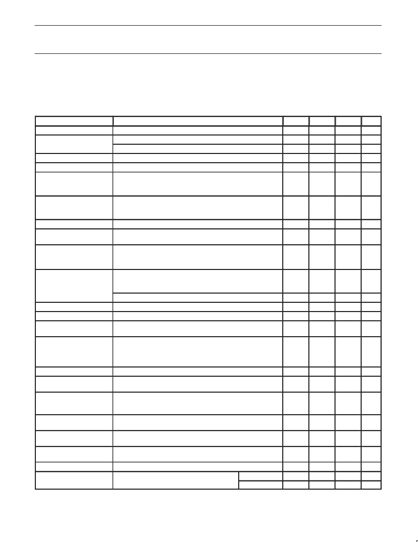
10. SA2400A TRANSMITTER
The IQ baseband input signal used is 11 Msymbols/sec QPSK with pulse shaping and 44 MHz D/A sampling rate. The source EVM is less than
3%. The LO frequency is the same as the Transmitter channel center frequency, as the transmit IF input is at 0 Hz.
Table 8. SA2400A Transmitter properties
T
amb
= 25
°
C; V
CC
= 3.3 V.
Specification
Conditions
Min
Typ
Max
Units
RF output frequency
Typical
2.4
–
2.5
GHz
RF output power incl balun,
for a CCK modulated signal
Output1, maximum
4.5
8.0
–
dBm
Output2, maximum
–5
–1.5
–
dBm
Gain step size
Output1 and Output2
–
1
–
dB
# gain steps
Output1 and Output2
–
15
–
Spectral Mask (Output1)
Note 1.
–11 to + 11 MHz, 100 kHz band
–22 to –11 and 11 to 22 MHz, 100 kHz band
< –22, > 22 MHz, 100 kHz band
–11 to + 11 MHz, 100 kHz band
–22 to –11 and 11 to 22 MHz, 100 kHz band
< –22, > 22 MHz, 100 kHz band
10% to 90% ramp up.
–
–
–
–
–
–
–
–
–40
–60
–
–
–
0.5
0
–36
–56
0
–30
–50
–
dBc
dBc
dBc
dBc
dBc
dBc
μ
s
μ
s
Spectral Mask (Output2)
Note 1.
Power ramping up time
Note 2.
Power ramping up delay
(Note 3)
From programming to TRANSMIT mode (TXRX mode, or 0-to-1
change of TX/RX pin).
Note 2.
–
2
–
Power ramping down
Note 2.
a) 90% to 10% ramp down
b) 10% to carrier leakage level
Analog input mode selected. No signal input, only quiescent current.
a) Uncalibrated
b) Calibrated
Digital input mode selected.
–
–
0.5
0.5
–
–
μ
s
μ
s
Carrier Leakage
–
–
–
–
–40
–40
–25
–30
–28
dBc
dBc
dBc
μ
A
dB
Carrier Leakage Adjustment
Adjustment range of input current offset
–10
–
+10
Residual Sideband Rejection
Includes both IQ phase and gain imbalance
22
–
–
Error Vector Magnitude
11 Msymbols/s QPSK. Both RF outputs. Measured with maximum
gain. Note 2.
–
12
14
%
RX to TX switching time
Note 2.
a) Output power within 1 dB of final value. Includes 2.5
μ
s for
power-up delay and ramping.
b) Frequency step settles to within 25 ppm of final value
Upper 3 dB cut off frequency, after calibration.
–
3
3.5
s
–
9.25
3
9.75
3.5
10.25
μ
s
MHz
IQ filter bandwidth
Note 2.
In-band IQ Common Mode
Rejection Ratio
1–6 MHz common mode signal at –30 dBc relative to IQ differential
signal. Measured at upconverted transmitter output.
Note 2.
30
–
–
dB
Out-of-band IQ Common
Mode Rejection Ratio
22–100 MHz common mode signal at –10 dBc relative to IQ
differential signal. Measured at upconverted transmitter output
relative to in-band 1 MHz tone.
Note 2.
40
–
–
dB
IQ input signal current range
Into each arm of differential inputs that sink current to ground.
Analog input selected. Note 4.
50
–
550
μ
A
IQ input quiescent current
Into each arm of differential inputs that sink current to ground.
Analog input selected.
–
300
–
μ
A
Resulting I/Q bias voltage
With 300
μ
A quiescent current into each arm of differential inputs.
Analog input selected.
0.6
0.7
0.8
V
IQ AC input impedance
Analog input selected.
–
320
–
V
IQ input voltage
Digital input selected
Logic LOW
–
–
0.2V
DD
–
Logic HIGH
0.8V
DD
–
V
相關(guān)PDF資料 |
PDF描述 |
|---|---|
| SA2400ABE | Single chip transceiver for 2.45 GHz ISM band |
| SA5522 | 1.4 GHz I2C-bus controlled synthesizer |
| SA572F | Programmable analog compandor |
| SAA2013HB-S | Digital Audio Tape Circuit |
| SAA2500GP | Video Processing/ENDEC for MPEG |
相關(guān)代理商/技術(shù)參數(shù) |
參數(shù)描述 |
|---|---|
| SA2400ABE | 制造商:PHILIPS 制造商全稱:NXP Semiconductors 功能描述:Single chip transceiver for 2.45 GHz ISM band |
| SA2403 | 功能描述:標(biāo)準(zhǔn)環(huán)形連接器 CIRCULAR MALE CONN 3 POLE RoHS:否 制造商:Hirose Connector 系列:EM-W 產(chǎn)品類型:Accessories 位置/觸點(diǎn)數(shù)量:1 觸點(diǎn)類型: 觸點(diǎn)電鍍: 安裝風(fēng)格:Cable 外殼材質(zhì): 端接類型:Clamp 電壓額定值: |
| SA2403(3POLE) | 制造商:BULGIN 制造商全稱:BULGIN 功能描述:Plugs and Sockets (3 & 4 pole) |
| SA2404 | 功能描述:標(biāo)準(zhǔn)環(huán)形連接器 CIRCULAR FEMALE CONN OUTLET 3 POLE RoHS:否 制造商:Hirose Connector 系列:EM-W 產(chǎn)品類型:Accessories 位置/觸點(diǎn)數(shù)量:1 觸點(diǎn)類型: 觸點(diǎn)電鍍: 安裝風(fēng)格:Cable 外殼材質(zhì): 端接類型:Clamp 電壓額定值: |
| SA2404(3POLE) | 制造商:BULGIN 制造商全稱:BULGIN 功能描述:Plugs and Sockets (3 & 4 pole) |
發(fā)布緊急采購,3分鐘左右您將得到回復(fù)。