- 您現(xiàn)在的位置:買賣IC網(wǎng) > PDF目錄372063 > RJ80530VZ733256 Microprocessor PDF資料下載
參數(shù)資料
| 型號: | RJ80530VZ733256 |
| 英文描述: | Microprocessor |
| 中文描述: | 微處理器 |
| 文件頁數(shù): | 25/89頁 |
| 文件大小: | 1672K |
| 代理商: | RJ80530VZ733256 |
第1頁第2頁第3頁第4頁第5頁第6頁第7頁第8頁第9頁第10頁第11頁第12頁第13頁第14頁第15頁第16頁第17頁第18頁第19頁第20頁第21頁第22頁第23頁第24頁當前第25頁第26頁第27頁第28頁第29頁第30頁第31頁第32頁第33頁第34頁第35頁第36頁第37頁第38頁第39頁第40頁第41頁第42頁第43頁第44頁第45頁第46頁第47頁第48頁第49頁第50頁第51頁第52頁第53頁第54頁第55頁第56頁第57頁第58頁第59頁第60頁第61頁第62頁第63頁第64頁第65頁第66頁第67頁第68頁第69頁第70頁第71頁第72頁第73頁第74頁第75頁第76頁第77頁第78頁第79頁第80頁第81頁第82頁第83頁第84頁第85頁第86頁第87頁第88頁第89頁
Mobile Intel
Pentium
III Processor-M Datasheet
298340-002
Datasheet
25
specific to the opposite operating mode. The timing specifications must be met when performing an
operating mode transition
.
3.5
Maximum Ratings
Table 8 contains the Mobile Intel Pentium
III
Processor-M stress ratings. Functional operation at the
absolute maximum and minimum is neither implied nor guaranteed. The processor should not receive a
clock while subjected to these conditions. Functional operating conditions are provided in the AC and
DC tables. Extended exposure to the maximum ratings may affect device reliability. Furthermore,
although the processor contains protective circuitry to resist damage from static electric discharge, one
should always take precautions to avoid high static voltages or electric fields.
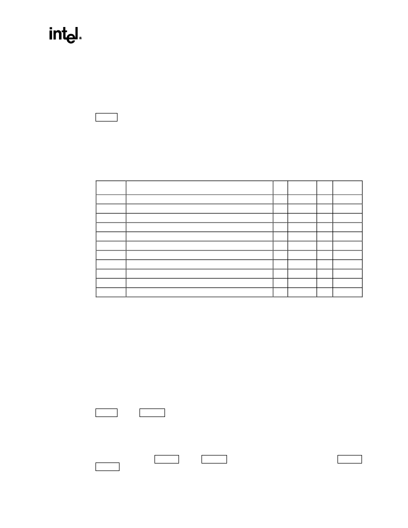
Table 8. Mobile Intel Pentium III Processor-M Absolute Maximum Ratings
Symbol
Parameter
Min
Max
Unit
Notes
T
Storage
Storage Temperature
–40 85
°C
Note 1
V
CC
(Abs)
Supply Voltage with respect to V
SS
–0.5 1.75
V
V
CCT
System Bus Buffer Voltage with respect to V
SS
–0.3 1.75
V
V
IN GTL
System Bus Buffer DC Input Voltage with respect to V
SS
–0.3 1.75
V
Notes 2, 3
V
IN125
1.25V Buffer DC Input Voltage with respect to V
SS
–0.3 1.75
V
Note 4
V
IN15
1.5V Buffer DC Input Voltage with respect to V
SS
–0.3 2.0
V
Note 5
V
IN18
1.8V Buffer DC Input Voltage with respect to V
SS
–0.3 2.0
V
Note 6
V
IN20
2.0V Buffer DC Input Voltage with respect to V
SS
–0.3 2.4
V
Note 7
V
IN25
2.5V Buffer DC Input Voltage with respect to V
SS
–0.3 3.3
V
Note 9
V
INVID
VID ball/pin DC Input Voltage with respect to V
SS
—
3.465
V
Note 8
I
VID
NOTES:
1.
The shipping container is only rated for 65°C.
2.
Parameter applies to the AGTL signal groups only. Compliance with both V
IN GTL
specifications is required.
3.
The voltage on the AGTL signals must never be below –0.3 or above 1.75V with respect to ground.
4.
Parameter applies to CLKREF, GHI#, TESTHI, VTTPWRGD signals.
5.
Parameter applies to CMOS, Open-drain, APIC, TESTLO and TAP bus signal groups only.
6.
Parameter applies to PWRGOOD signal.
7.
Parameter applies to PICCLK signal.
8.
Parameter applies to each VID pin/ball individually.
9.
Parameter applies to BCLK signal in Single Ended Clocking Mode.
VID Current
-0.3 3.6
mA
Note 8
3.6
DC Specifications
Table 9 through Table 18 list the DC specifications for the Mobile Intel Pentium
III
Processor-M.
Specifications are valid only while meeting specifications for the junction temperature, clock
frequency, and input voltages. The junction temperature range for all DC specifications is 0°C to
100°C. Care should be taken to read all notes associated with each parameter. Unlike the mobile
Pentium
III
processor, the V
cc
tolerances for the Mobile Intel Pentium
III
Processor-M are not specified
as a percentage of nominal. The tolerances are instead specified in the form of load lines for the static
and transient cases in Table 10 through Table 15. Illustration of the load lines is shown in Figure 4 and
Figure 5.
相關PDF資料 |
PDF描述 |
|---|---|
| RHFL4913 | THREE-TERMINAL POSITIVE FIXED VOLTAGE REGULATORS |
| RHFL4913S50-04V | THREE-TERMINAL POSITIVE FIXED VOLTAGE REGULATORS |
| RHFL4913ESY5005V | Converta Box Enclosure; Enclosure Material:Aluminum; External Height:2"; External Width:8"; External Depth:4"; Enclosure Color:Natural |
| RHFL4913ESY3305V | Standard Recovery Rectifier; Forward Current:20A; Forward Current Average:12.7A; Forward Current Avg Rectified, IF(AV):12.7A; Forward Surge Current Max, Ifsm:300A; Forward Voltage:1.1V; Forward Voltage Max, VF:1.1V RoHS Compliant: Yes |
| RHFL4913ESY3306V | Standard Recovery Rectifier; Forward Current:20A; Forward Current Average:12.7A; Forward Current Avg Rectified, IF(AV):12.7A; Forward Surge Current Max, Ifsm:300A; Forward Voltage:1.1V; Forward Voltage Max, VF:1.1V RoHS Compliant: Yes |
相關代理商/技術參數(shù) |
參數(shù)描述 |
|---|---|
| RJ80530VZ800256 | 制造商:Rochester Electronics LLC 功能描述:- Bulk |
| RJ80535GC0171M | 制造商:Rochester Electronics LLC 功能描述:MOBILE PENTIUM M,1.4GHZ,1M,UFCBGA - Bulk 制造商:Intel 功能描述: |
| RJ80535GC0171M S L6F5 | 制造商:Intel 功能描述:MPU Pentium? M Processor RISC 32-Bit 130nm 1.4GHz 479-Pin HPBGA Tray 制造商:Intel 功能描述:PENTIUM M PROCESSOR 1.40 GHZ |
| RJ80535GC0211M | 制造商:Intel 功能描述: |
| RJ80535GC0251M | 制造商:Rochester Electronics LLC 功能描述:MOBILE PENTIUM M,1.6GHZ,1M,UFCBGA - Bulk |
發(fā)布緊急采購,3分鐘左右您將得到回復。