- 您現(xiàn)在的位置:買賣IC網(wǎng) > PDF目錄370849 > M37736EHBGS (Mitsubishi Electric Corporation) PROM VERSION OF M37736EHBXXXGP PDF資料下載
參數(shù)資料
| 型號(hào): | M37736EHBGS |
| 廠商: | Mitsubishi Electric Corporation |
| 英文描述: | PROM VERSION OF M37736EHBXXXGP |
| 中文描述: | PROM的版本M37736EHBXXXGP |
| 文件頁(yè)數(shù): | 59/96頁(yè) |
| 文件大小: | 1328K |
| 代理商: | M37736EHBGS |
第1頁(yè)第2頁(yè)第3頁(yè)第4頁(yè)第5頁(yè)第6頁(yè)第7頁(yè)第8頁(yè)第9頁(yè)第10頁(yè)第11頁(yè)第12頁(yè)第13頁(yè)第14頁(yè)第15頁(yè)第16頁(yè)第17頁(yè)第18頁(yè)第19頁(yè)第20頁(yè)第21頁(yè)第22頁(yè)第23頁(yè)第24頁(yè)第25頁(yè)第26頁(yè)第27頁(yè)第28頁(yè)第29頁(yè)第30頁(yè)第31頁(yè)第32頁(yè)第33頁(yè)第34頁(yè)第35頁(yè)第36頁(yè)第37頁(yè)第38頁(yè)第39頁(yè)第40頁(yè)第41頁(yè)第42頁(yè)第43頁(yè)第44頁(yè)第45頁(yè)第46頁(yè)第47頁(yè)第48頁(yè)第49頁(yè)第50頁(yè)第51頁(yè)第52頁(yè)第53頁(yè)第54頁(yè)第55頁(yè)第56頁(yè)第57頁(yè)第58頁(yè)當(dāng)前第59頁(yè)第60頁(yè)第61頁(yè)第62頁(yè)第63頁(yè)第64頁(yè)第65頁(yè)第66頁(yè)第67頁(yè)第68頁(yè)第69頁(yè)第70頁(yè)第71頁(yè)第72頁(yè)第73頁(yè)第74頁(yè)第75頁(yè)第76頁(yè)第77頁(yè)第78頁(yè)第79頁(yè)第80頁(yè)第81頁(yè)第82頁(yè)第83頁(yè)第84頁(yè)第85頁(yè)第86頁(yè)第87頁(yè)第88頁(yè)第89頁(yè)第90頁(yè)第91頁(yè)第92頁(yè)第93頁(yè)第94頁(yè)第95頁(yè)第96頁(yè)
59
PRELIMINARY
Notice: This is not a final specification.
Some parametric limits are subject to change.
MITSUBISHI MICROCOMPUTERS
M37736MHBXXXGP
SINGLE-CHIP 16-BIT CMOS MICROCOMPUTER
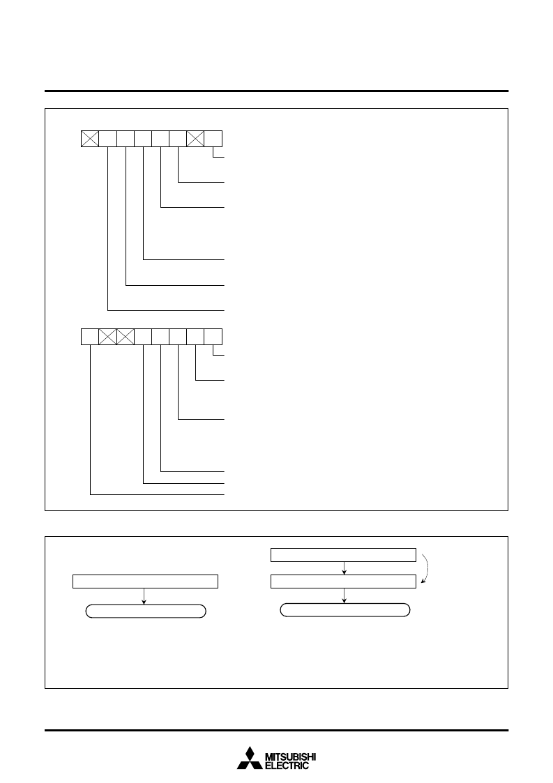
Oscillation circuit control register 0
X
drivability selection bit
0 : LOW
1 : HIGH
Main clock stop bit
0 : Main-clock oscillation is available.
1 : Main-clock oscillation is stopped.
System clock selection bit
Port-X
C
selection bit = “0” (Sub clock is not used.)
0 : Main clock is selected.
1 : Main clock divided by 8 is selected.
Port-X
selection bit = “1” (Sub clock is used.)
0 : Main clock is selected.
1 : Sub clock is selected.
Port-Xc selection bit
0 : Ports P7
7
and P7
6
are selected. (Sub clock is not used.)
1 : Pins X
CIN
and X
COUT
are selected. (Sub clock is used.)
System clock stop bit at wait state
0 : Clocks f
2
to f
512
are operating at WIT state
1 : Clocks f
2
to f
512
stop at WIT state
Signal output disable selection bit (Refer to Table 7.)
Address
6C
16
Note.
Write to the oscillation circuit control
register 1 as the flow shown in Figure 65.
CM
6
CM
5
CM
4
CM
3
CM
2
CM
0
7
6
5
4
3
2
1
0
Oscillation circuit control register 1
Main clock division selection bit
0 : Main clock is divided by 2.
1 : Main clock is not divided by 2.
Main clock external input selection bit
0 : Main-clock oscillation circuit is operating by itself.
Watchdog timer is used at returning from STP state.
1 : Main-clock is input externally.
Watchdog timer is not used at returning from STP state.
Sub clock external input selection bit
0 : Sub-clock oscillation circuit is operating by itself.
Port P7
functions as X
pin.
Watchdog timer is used at returning from STP state.
1 : Sub-clock is input externally.
Port P7
6
functions as I/O port.
Watchdog timer is not used ar returning from STP state.
X : Not used
0 : Always “0” (However, writing data “55
16
” shown in Figure 65 is possible.)
Clock prescaler reset bit
Address
6F
16
CC
0
CC
1
CC
2
0
7
6
5
4
3
2
1
0
Fig. 64 Bit configuration of oscillation circuit control registers 0, 1
Fig. 65 How to write data in oscillation circuit control register 1
Writing data “80
16
” (LDM instruction)
Reset clock prescaler
Writing data “55
16
” (LDM instruction)
Writing data “0Y
16
” (LDM instruction)
CC
2
to CC
0
selection bits
How to reset clock prescaler
How to write in CC
2
to CC
0
selection bits
Note.
“Y” is the sum of bits to be set. For example,
when
setting bits 2 and 1 to “1”, “Y” becomes “6”.
Next instruction
相關(guān)PDF資料 |
PDF描述 |
|---|---|
| M37736EHLXXXHP | PROM VERSION OF M37736MHLXXXHP(MICROCOMPUTERS) |
| M37736MHLXXXHP | SINGLE-CHIP 16-BIT CMOS MICROCOMPUTER |
| M37736EHBXXXGP | PROM VERSION OF M37736MHBXXXGP(MICROCOMPUTERS) |
| M37736MHBXXXGP | SINGLE-CHIP 16-BIT CMOS MICROCOMPUTER |
| M37753FFCFP | SINGLE CHIP 16 BIT CMOS MICROCOMPUTER FLASH MEMORY VERSION |
相關(guān)代理商/技術(shù)參數(shù) |
參數(shù)描述 |
|---|---|
| M37736EHBXXXGP | 制造商:MITSUBISHI 制造商全稱:Mitsubishi Electric Semiconductor 功能描述:PROM VERSION OF M37736MHBXXXGP(MICROCOMPUTERS) |
| M37736EHL | 制造商:MITSUBISHI 制造商全稱:Mitsubishi Electric Semiconductor 功能描述:PROM VERSION OF M37736MHLXXXHP(MICROCOMPUTERS) |
| M37736EHLXXXHP | 制造商:RENESAS 制造商全稱:Renesas Technology Corp 功能描述:PROM VERSION OF M37736MHLXXXHP |
| M37736M4B | 制造商:MITSUBISHI 制造商全稱:Mitsubishi Electric Semiconductor 功能描述:SINGLE-CHIP 16-BIT CMOS MICROCOMPUTER |
| M37736M4BXXXGP | 制造商:MITSUBISHI 制造商全稱:Mitsubishi Electric Semiconductor 功能描述:SINGLE-CHIP 16-BIT CMOS MICROCOMPUTER |
發(fā)布緊急采購(gòu),3分鐘左右您將得到回復(fù)。