- 您現(xiàn)在的位置:買賣IC網(wǎng) > PDF目錄44968 > LSM303DLHTR (STMICROELECTRONICS) SPECIALTY ANALOG CIRCUIT, PBGA28 PDF資料下載
參數(shù)資料
| 型號: | LSM303DLHTR |
| 廠商: | STMICROELECTRONICS |
| 元件分類: | 模擬信號調(diào)理 |
| 英文描述: | SPECIALTY ANALOG CIRCUIT, PBGA28 |
| 封裝: | 5 X 5 MM, 1 MM HEIGHT, ROHS COMPLIANT, PLASTIC, LGA-16 |
| 文件頁數(shù): | 18/47頁 |
| 文件大小: | 585K |
| 代理商: | LSM303DLHTR |
第1頁第2頁第3頁第4頁第5頁第6頁第7頁第8頁第9頁第10頁第11頁第12頁第13頁第14頁第15頁第16頁第17頁當前第18頁第19頁第20頁第21頁第22頁第23頁第24頁第25頁第26頁第27頁第28頁第29頁第30頁第31頁第32頁第33頁第34頁第35頁第36頁第37頁第38頁第39頁第40頁第41頁第42頁第43頁第44頁第45頁第46頁第47頁
LSM303DLH
Digital interfaces
Doc ID 16941 Rev 1
25/47
7.1.2
Linear acceleration digital interface
For linear acceleration, the default (factory) 7-bit slave address is 001100xb. The
SDO/SA0 pad can be used to modify the least significant bit of the device address. If the
SA0 pad is connected to voltage supply, LSb is ‘1’ (address 0011001b) otherwise if the SA0
pad is connected to ground, LSb value is ‘0’ (address 0011000b). This solution permits
connecting and addressing two different accelerometers to the same I2C lines.
The slave address is completed with a read/write bit. If the bit was ‘1’ (read), a repeated
START (SR) condition will have to be issued after the two sub-address bytes; if the bit is ‘0’
(write) the master transmits to the slave with direction unchanged.
Table 14 explains how
the SAD+Read/Write bit pattern is composed, listing all the possible configurations.
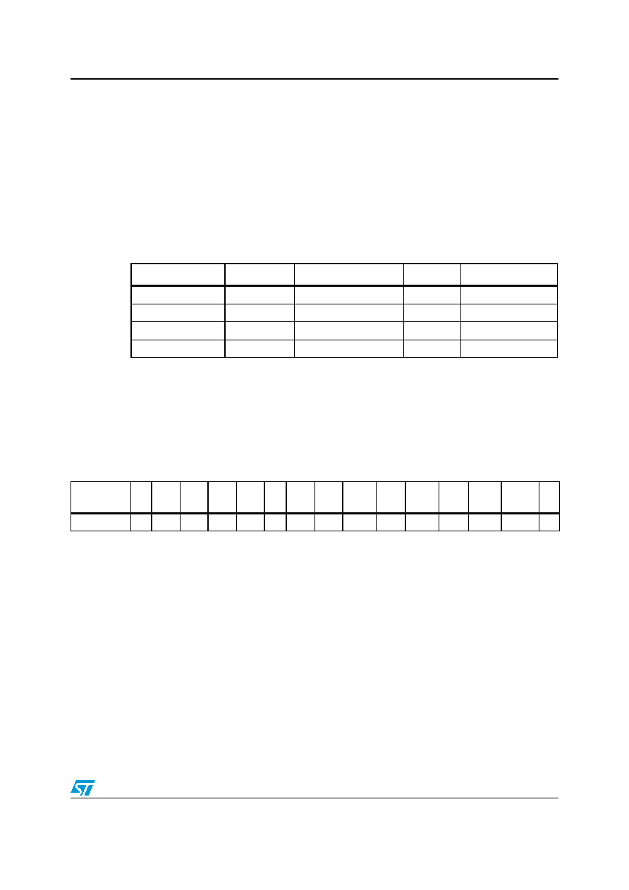
Table 14.
SAD+Read/Write patterns
In order to read multiple bytes, it is necessary to assert the most significant bit of the sub-
address field. In other words, SUB(7) must be equal to 1 while SUB(6-0) represents the
address of the first register to be read.
In the presented communication format , MAK is Master Acknowledge and NMAK is No
Master Acknowledge.
7.1.3
Magnetic field digital interface
The system communicates via a two-wire I2C bus system as a slave device. The interface
protocol is defined by the I2C bus specification. The data rate is the standard mode 100
kbps or 400 kbps rates as defined by the I2C bus specifications. The bus bit format is an 8-
bit data/address send and a 1-bit acknowledge bit. The format of the data bytes (payload)
shall be case-sensitive ASCII characters or binary data to the magnetic sensor slave, and
binary data returned. Negative binary values will be in two’s complement form.
For magnetic sensor, the default (factory) 7-bit slave address is 0011110b
(0x3C) for write operations, or 00111101b (0x3D) for read operations.
The Serial Clock (SCL_M) and Serial Data (SDA_M) lines have optional internal pull-up
resistors, but require resistive pull-up (Rp) between the master device (usually a host
microprocessor) and the LSM303DLH. Pull-up resistance values of about 10 k
are
recommended with a nominal 1.8 V digital supply voltage (Vdd_dig_M).
Command
SAD[6:1]
SAD[0] = SA0
R/W
SAD+R/W
Read
001100
0
1
00110001 (31h)
Write
001100
0
00110000 (30h)
Read
001100
1
00110011 (33h)
Write
001100
1
0
00110010 (32h)
Table 15.
Transfer when master is receiving (reading) multiple bytes of data from slave
Master
ST
SAD
+W
SUB
SR
SAD
+R
MAK
NMAK
SP
Slave
SAK
DATA
相關(guān)PDF資料 |
PDF描述 |
|---|---|
| LSM330DL | SPECIALTY ANALOG CIRCUIT, PBGA28 |
| LSN-0.75/16-D12HJ-C | 1-OUTPUT 12.8 W DC-DC REG PWR SUPPLY MODULE |
| LSN-1.8/16-D12HJ-C | 1-OUTPUT 28.8 W DC-DC REG PWR SUPPLY MODULE |
| LSN-1.2/16-D12HJ-C | 1-OUTPUT 19.2 W DC-DC REG PWR SUPPLY MODULE |
| LSN-2.5/16-D12HJ-C | 1-OUTPUT 40 W DC-DC REG PWR SUPPLY MODULE |
相關(guān)代理商/技術(shù)參數(shù) |
參數(shù)描述 |
|---|---|
| LSM303DLM | 功能描述:加速計 - 板上安裝 3axis accelerometr & 3-axis magnetometer RoHS:否 制造商:Murata 傳感軸:Double 加速:12 g 靈敏度: 封裝 / 箱體: 輸出類型:Analog 數(shù)字輸出 - 位數(shù):11 bit 電源電壓-最大:5.25 V 電源電壓-最小:4.75 V 電源電流:4 mA 最大工作溫度:+ 125 C 最小工作溫度:- 40 C |
| LSM303DLMTR | 功能描述:加速計 - 板上安裝 3-Axis 2.16V to 3.6V 3D Magnetic 3-Ch RoHS:否 制造商:Murata 傳感軸:Double 加速:12 g 靈敏度: 封裝 / 箱體: 輸出類型:Analog 數(shù)字輸出 - 位數(shù):11 bit 電源電壓-最大:5.25 V 電源電壓-最小:4.75 V 電源電流:4 mA 最大工作溫度:+ 125 C 最小工作溫度:- 40 C |
| LSM303DLMTR-CUT TAPE | 制造商:ST 功能描述:LSM303DLM Series 3 Axis ?/?/? g 3.6 V Digital Output Accelerometer - LGA-28L |
| LSM303DTR | 功能描述:加速計 - 板上安裝 Ultra Compact High Perf E-Compass 3D accelerometer and 3D magnetometer module RoHS:否 制造商:Murata 傳感軸:Double 加速:12 g 靈敏度: 封裝 / 箱體: 輸出類型:Analog 數(shù)字輸出 - 位數(shù):11 bit 電源電壓-最大:5.25 V 電源電壓-最小:4.75 V 電源電流:4 mA 最大工作溫度:+ 125 C 最小工作溫度:- 40 C |
| LSM315 | 制造商:MICROSEMI 制造商全稱:Microsemi Corporation 功能描述:3 AMP SCHOTTKY ORING RECTIFIER |
發(fā)布緊急采購,3分鐘左右您將得到回復(fù)。