- 您現(xiàn)在的位置:買賣IC網(wǎng) > PDF目錄385472 > LH79524N0F100A1 (NXP Semiconductors N.V.) System-on-Chip PDF資料下載
參數(shù)資料
| 型號(hào): | LH79524N0F100A1 |
| 廠商: | NXP Semiconductors N.V. |
| 元件分類: | 數(shù)學(xué)處理器 |
| 英文描述: | System-on-Chip |
| 封裝: | LH79524N0F100A1<SOT1019-1 (LFBGA208)|<<http://www.nxp.com/packages/SOT1019-1.html<1<Always Pb-free,;LH79525N0Q100A1<SOT1017-1 (LQFP176)|<<http://www.nxp.com/packages/SOT1 |
| 文件頁數(shù): | 32/64頁 |
| 文件大小: | 970K |
| 代理商: | LH79524N0F100A1 |
第1頁第2頁第3頁第4頁第5頁第6頁第7頁第8頁第9頁第10頁第11頁第12頁第13頁第14頁第15頁第16頁第17頁第18頁第19頁第20頁第21頁第22頁第23頁第24頁第25頁第26頁第27頁第28頁第29頁第30頁第31頁當(dāng)前第32頁第33頁第34頁第35頁第36頁第37頁第38頁第39頁第40頁第41頁第42頁第43頁第44頁第45頁第46頁第47頁第48頁第49頁第50頁第51頁第52頁第53頁第54頁第55頁第56頁第57頁第58頁第59頁第60頁第61頁第62頁第63頁第64頁
LH79524/LH79525
System-on-Chip
32
Rev. 01
—
16 July 2007
Preliminary data sheet
NXP Semiconductors
Analog-To-Digital Converter
Electrical Characteristics
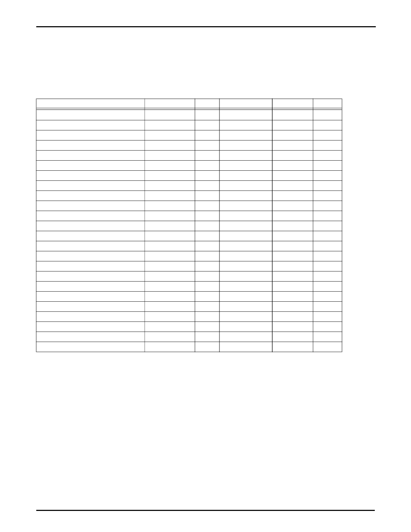
Table 15 shows the ADC electrical characteristics.
See Figure 10 for the ADC transfer characteristics.
NOTES:
1. The analog section of the ADC takes 16 × A2DCLK cycles per conversion plus 1 × A2DCLK cycles to be made available in the PCLK
domain. An additional 3 × PCLK cycles are required before being available on the APB.
2. The internal voltage reference is driven to nominal value VREF = 2.0 V. Using the Reference Multiplexer, alternative low impedance
(RS < 500) voltages can be selected as reference voltages. The range of voltages allowed are specified above. However, the on-chip
reference cannot drive the ADC unless the reference buffer is switched on.
3. The analog input pins can be driven anywhere between the power supply rails. If the voltage at the input to the ADC exceeds VREF+
or is below VREF-, the A/D result will saturate appropriately at positive or negative full scale. Trying to pull the analog input pins above
or below the power supply rails will cause protection diodes to be forward-biased, resulting in large current source/sink and possible
damage to the ADC.
4. Bandgap and other low-bandwidth circuitry operating. All other ADC blocks shut down.
Table 15. ADC Electrical Characteristics
PARAMETER
MIN.
TYP.
MAX.
UNITS
NOTES
A/D Resolution
10
10
Bits
Throughput Conversion
17
CLK Cycles
1
Acquisition Time
3
CLK Cycles
Data Format
binary
CLK Frequency
500
5,000
ns
Differential Non-Linearity
-0.99
3.0
LSB
Integral Non-Linearity
-3.0
+3.0
LSB
Offset Error
-10
+10
mV
Gain Error
-2.0
+2.0
LSB
Reference Voltage Output
1.85
2.0
2.15
V
VREF-
VSSA
VSSA
(VREF+) -1.0 V
V
2
VREF+
(VREF-) +1.0 V
VREF
VDDA
V
2
Crosstalk between channels
-60
dB
Analog Input Voltage Range
0
VDDA
V
μ
A
μ
A
3
Analog Input Current
5
Reference Input Current
5
Analog input capacitance
15
pF
Operating Supply Voltage
3.0
3.6
V
μ
A
μ
A
μ
A
Operating Current, VDDA0
590
1000
Powerdown Current, VDDA0
1
10
Standby Current
180
300
4
Brown Out Trip Point (falling point)
2.36
2.63
2.9
V
Brown Out Hysterisis
120
mV
Operating Temperature
-40
85
°C
相關(guān)PDF資料 |
PDF描述 |
|---|---|
| LH79525N0Q100A1 | System-on-Chip |
| LH7A400N0F000B5 | 32-Bit System-on-Chip |
| LH7A400N0F076B5 | 32-Bit System-on-Chip |
| LH7A400N0G000B5 | 32-Bit System-on-Chip |
| LH7A404N0F000B3 | 32-Bit System-on-Chip |
相關(guān)代理商/技術(shù)參數(shù) |
參數(shù)描述 |
|---|---|
| LH79524N0F100A1,55 | 功能描述:ARM微控制器 - MCU LCD,USB,ETH’NET,MMU,ADC,BGA208 RoHS:否 制造商:STMicroelectronics 核心:ARM Cortex M4F 處理器系列:STM32F373xx 數(shù)據(jù)總線寬度:32 bit 最大時(shí)鐘頻率:72 MHz 程序存儲(chǔ)器大小:256 KB 數(shù)據(jù) RAM 大小:32 KB 片上 ADC:Yes 工作電源電壓:1.65 V to 3.6 V, 2 V to 3.6 V, 2.2 V to 3.6 V 工作溫度范圍:- 40 C to + 85 C 封裝 / 箱體:LQFP-48 安裝風(fēng)格:SMD/SMT |
| LH79524N0F100A1,551 | 制造商:NXP Semiconductors 功能描述: |
| LH79524N0F100A1;55 | 功能描述:ARM微控制器 - MCU LCD USB ETH’NET MMU RoHS:否 制造商:STMicroelectronics 核心:ARM Cortex M4F 處理器系列:STM32F373xx 數(shù)據(jù)總線寬度:32 bit 最大時(shí)鐘頻率:72 MHz 程序存儲(chǔ)器大小:256 KB 數(shù)據(jù) RAM 大小:32 KB 片上 ADC:Yes 工作電源電壓:1.65 V to 3.6 V, 2 V to 3.6 V, 2.2 V to 3.6 V 工作溫度范圍:- 40 C to + 85 C 封裝 / 箱體:LQFP-48 安裝風(fēng)格:SMD/SMT |
| LH79524N0F100A1-S | 功能描述:ARM微控制器 - MCU ARM7 LCD MMU ENET RoHS:否 制造商:STMicroelectronics 核心:ARM Cortex M4F 處理器系列:STM32F373xx 數(shù)據(jù)總線寬度:32 bit 最大時(shí)鐘頻率:72 MHz 程序存儲(chǔ)器大小:256 KB 數(shù)據(jù) RAM 大小:32 KB 片上 ADC:Yes 工作電源電壓:1.65 V to 3.6 V, 2 V to 3.6 V, 2.2 V to 3.6 V 工作溫度范圍:- 40 C to + 85 C 封裝 / 箱體:LQFP-48 安裝風(fēng)格:SMD/SMT |
| LH79525 | 制造商:PHILIPS 制造商全稱:NXP Semiconductors 功能描述:System-on-Chip |
發(fā)布緊急采購,3分鐘左右您將得到回復(fù)。