- 您現(xiàn)在的位置:買賣IC網(wǎng) > PDF目錄299403 > LFXP15C-4FN256C (LATTICE SEMICONDUCTOR CORP) PDF資料下載
參數(shù)資料
| 型號(hào): | LFXP15C-4FN256C |
| 廠商: | LATTICE SEMICONDUCTOR CORP |
| 元件分類: | FPGA |
| 中文描述: | FPGA, 1932 CLBS, PBGA256 |
| 封裝: | 17 X 17 MM, LEAD FREE, FPBGA-256 |
| 文件頁數(shù): | 98/130頁 |
| 文件大小: | 1312K |
| 代理商: | LFXP15C-4FN256C |
第1頁第2頁第3頁第4頁第5頁第6頁第7頁第8頁第9頁第10頁第11頁第12頁第13頁第14頁第15頁第16頁第17頁第18頁第19頁第20頁第21頁第22頁第23頁第24頁第25頁第26頁第27頁第28頁第29頁第30頁第31頁第32頁第33頁第34頁第35頁第36頁第37頁第38頁第39頁第40頁第41頁第42頁第43頁第44頁第45頁第46頁第47頁第48頁第49頁第50頁第51頁第52頁第53頁第54頁第55頁第56頁第57頁第58頁第59頁第60頁第61頁第62頁第63頁第64頁第65頁第66頁第67頁第68頁第69頁第70頁第71頁第72頁第73頁第74頁第75頁第76頁第77頁第78頁第79頁第80頁第81頁第82頁第83頁第84頁第85頁第86頁第87頁第88頁第89頁第90頁第91頁第92頁第93頁第94頁第95頁第96頁第97頁當(dāng)前第98頁第99頁第100頁第101頁第102頁第103頁第104頁第105頁第106頁第107頁第108頁第109頁第110頁第111頁第112頁第113頁第114頁第115頁第116頁第117頁第118頁第119頁第120頁第121頁第122頁第123頁第124頁第125頁第126頁第127頁第128頁第129頁第130頁
2-4
Architecture
Lattice Semiconductor
LatticeXP Family Data Sheet
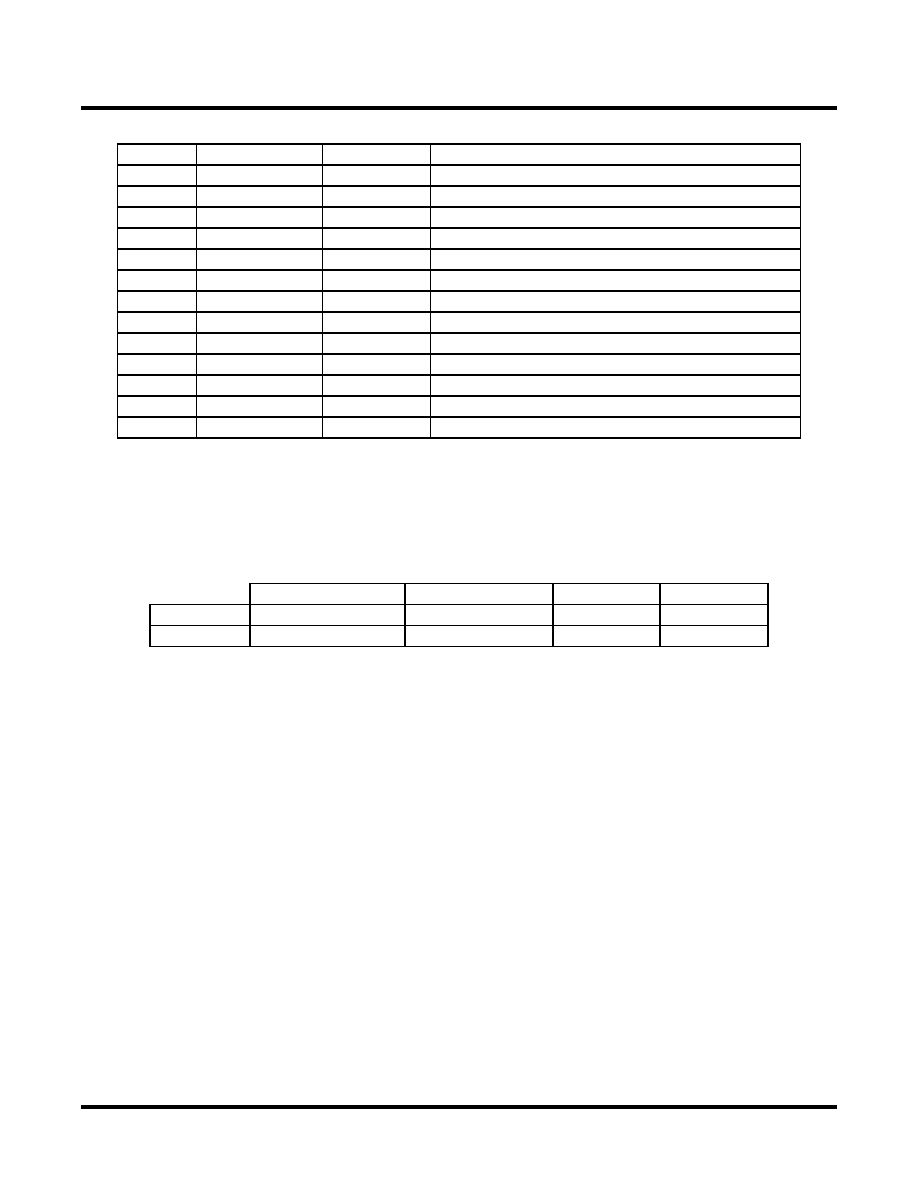
Table 2-1. Slice Signal Descriptions
Modes of Operation
Each Slice is capable of four modes of operation: Logic, Ripple, RAM and ROM. The Slice in the PFF is capable of
all modes except RAM. Table 2-2 lists the modes and the capability of the Slice blocks.
Table 2-2. Slice Modes
Logic Mode: In this mode, the LUTs in each Slice are configured as 4-input combinatorial lookup tables. A LUT4
can have 16 possible input combinations. Any logic function with four inputs can be generated by programming this
lookup table. Since there are two LUT4s per Slice, a LUT5 can be constructed within one Slice. Larger lookup
tables such as LUT6, LUT7 and LUT8 can be constructed by concatenating other Slices.
Ripple Mode: Ripple mode allows the efficient implementation of small arithmetic functions. In ripple mode, the fol-
lowing functions can be implemented by each Slice:
Addition 2-bit
Subtraction 2-bit
Add/Subtract 2-bit using dynamic control
Up counter 2-bit
Down counter 2-bit
Ripple mode multiplier building block
Comparator functions of A and B inputs
- A greater-than-or-equal-to B
- A not-equal-to B
- A less-than-or-equal-to B
Two additional signals: Carry Generate and Carry Propagate are generated per Slice in this mode, allowing fast
arithmetic functions to be constructed by concatenating Slices.
RAM Mode: In this mode, distributed RAM can be constructed using each LUT block as a 16x1-bit memory.
Through the combination of LUTs and Slices, a variety of different memories can be constructed.
Function
Type
Signal Names
Description
Input
Data signal
A0, B0, C0, D0 Inputs to LUT4
Input
Data signal
A1, B1, C1, D1 Inputs to LUT4
Input
Multi-purpose
M0
Multipurpose Input
Input
Multi-purpose
M1
Multipurpose Input
Input
Control signal
CE
Clock Enable
Input
Control signal
LSR
Local Set/Reset
Input
Control signal
CLK
System Clock
Input
Inter-PFU signal
FCIN
Fast Carry In
1
Output
Data signals
F0, F1
LUT4 output register bypass signals
Output
Data signals
Q0, Q1
Register Outputs
Output
Data signals
OFX0
Output of a LUT5 MUX
Output
Data signals
OFX1
Output of a LUT6, LUT7, LUT8
2 MUX depending on the slice
Output
Inter-PFU signal
FCO
For the right most PFU the fast carry chain output
1
1. See Figure 2-2 for connection details.
2. Requires two PFUs.
Logic
Ripple
RAM
ROM
PFU Slice
LUT 4x2 or LUT 5x1
2-bit Arithmetic Unit
SP 16x2
ROM 16x1 x 2
PFF Slice
LUT 4x2 or LUT 5x1
2-bit Arithmetic Unit
N/A
ROM 16x1 x 2
相關(guān)PDF資料 |
PDF描述 |
|---|---|
| LFZ3508VXX | GENERAL PURPOSE INDUCTOR |
| LFZ2805HXX | GENERAL PURPOSE INDUCTOR |
| LF02004VTX | GENERAL PURPOSE INDUCTOR |
| LG3341-NE7501 | T-1 SINGLE COLOR LED, GREEN, 3 mm |
| LG3341-KNE9117 | T-1 SINGLE COLOR LED, GREEN, 3 mm |
相關(guān)代理商/技術(shù)參數(shù) |
參數(shù)描述 |
|---|---|
| LFXP15C-4FN256I | 功能描述:FPGA - 現(xiàn)場(chǎng)可編程門陣列 15.4K LUTs 188 IO 1. 8/2.5/3.3V-4 Spd I RoHS:否 制造商:Altera Corporation 系列:Cyclone V E 柵極數(shù)量: 邏輯塊數(shù)量:943 內(nèi)嵌式塊RAM - EBR:1956 kbit 輸入/輸出端數(shù)量:128 最大工作頻率:800 MHz 工作電源電壓:1.1 V 最大工作溫度:+ 70 C 安裝風(fēng)格:SMD/SMT 封裝 / 箱體:FBGA-256 |
| LFXP15C-4FN388C | 功能描述:FPGA - 現(xiàn)場(chǎng)可編程門陣列 15.4K LUTs 268 IO 1. 8/2.5/3.3V -4 Spd RoHS:否 制造商:Altera Corporation 系列:Cyclone V E 柵極數(shù)量: 邏輯塊數(shù)量:943 內(nèi)嵌式塊RAM - EBR:1956 kbit 輸入/輸出端數(shù)量:128 最大工作頻率:800 MHz 工作電源電壓:1.1 V 最大工作溫度:+ 70 C 安裝風(fēng)格:SMD/SMT 封裝 / 箱體:FBGA-256 |
| LFXP15C-4FN388I | 功能描述:FPGA - 現(xiàn)場(chǎng)可編程門陣列 15.4K LUTs 268 IO 1. 8/2.5/3.3V-4 Spd I RoHS:否 制造商:Altera Corporation 系列:Cyclone V E 柵極數(shù)量: 邏輯塊數(shù)量:943 內(nèi)嵌式塊RAM - EBR:1956 kbit 輸入/輸出端數(shù)量:128 最大工作頻率:800 MHz 工作電源電壓:1.1 V 最大工作溫度:+ 70 C 安裝風(fēng)格:SMD/SMT 封裝 / 箱體:FBGA-256 |
| LFXP15C-4FN484C | 功能描述:FPGA - 現(xiàn)場(chǎng)可編程門陣列 15.4K LUTs 1.8/2.5/3 .3V -4 Spd RoHS:否 制造商:Altera Corporation 系列:Cyclone V E 柵極數(shù)量: 邏輯塊數(shù)量:943 內(nèi)嵌式塊RAM - EBR:1956 kbit 輸入/輸出端數(shù)量:128 最大工作頻率:800 MHz 工作電源電壓:1.1 V 最大工作溫度:+ 70 C 安裝風(fēng)格:SMD/SMT 封裝 / 箱體:FBGA-256 |
| LFXP15C-4FN484I | 功能描述:FPGA - 現(xiàn)場(chǎng)可編程門陣列 15.4K LUTs 1.8/2.5/3 .3V-4 Spd I RoHS:否 制造商:Altera Corporation 系列:Cyclone V E 柵極數(shù)量: 邏輯塊數(shù)量:943 內(nèi)嵌式塊RAM - EBR:1956 kbit 輸入/輸出端數(shù)量:128 最大工作頻率:800 MHz 工作電源電壓:1.1 V 最大工作溫度:+ 70 C 安裝風(fēng)格:SMD/SMT 封裝 / 箱體:FBGA-256 |
發(fā)布緊急采購(gòu),3分鐘左右您將得到回復(fù)。