- 您現(xiàn)在的位置:買賣IC網(wǎng) > PDF目錄299403 > LFXP15C-4FN256C (LATTICE SEMICONDUCTOR CORP) PDF資料下載
參數(shù)資料
| 型號(hào): | LFXP15C-4FN256C |
| 廠商: | LATTICE SEMICONDUCTOR CORP |
| 元件分類: | FPGA |
| 中文描述: | FPGA, 1932 CLBS, PBGA256 |
| 封裝: | 17 X 17 MM, LEAD FREE, FPBGA-256 |
| 文件頁數(shù): | 51/130頁 |
| 文件大小: | 1312K |
| 代理商: | LFXP15C-4FN256C |
第1頁第2頁第3頁第4頁第5頁第6頁第7頁第8頁第9頁第10頁第11頁第12頁第13頁第14頁第15頁第16頁第17頁第18頁第19頁第20頁第21頁第22頁第23頁第24頁第25頁第26頁第27頁第28頁第29頁第30頁第31頁第32頁第33頁第34頁第35頁第36頁第37頁第38頁第39頁第40頁第41頁第42頁第43頁第44頁第45頁第46頁第47頁第48頁第49頁第50頁當(dāng)前第51頁第52頁第53頁第54頁第55頁第56頁第57頁第58頁第59頁第60頁第61頁第62頁第63頁第64頁第65頁第66頁第67頁第68頁第69頁第70頁第71頁第72頁第73頁第74頁第75頁第76頁第77頁第78頁第79頁第80頁第81頁第82頁第83頁第84頁第85頁第86頁第87頁第88頁第89頁第90頁第91頁第92頁第93頁第94頁第95頁第96頁第97頁第98頁第99頁第100頁第101頁第102頁第103頁第104頁第105頁第106頁第107頁第108頁第109頁第110頁第111頁第112頁第113頁第114頁第115頁第116頁第117頁第118頁第119頁第120頁第121頁第122頁第123頁第124頁第125頁第126頁第127頁第128頁第129頁第130頁
2-24
Architecture
Lattice Semiconductor
LatticeXP Family Data Sheet
Typical I/O Behavior During Power-up
The internal power-on-reset (POR) signal is deactivated when VCC and VCCAUX have reached satisfactory levels.
After the POR signal is deactivated, the FPGA core logic becomes active. It is the user’s responsibility to ensure
that all other VCCIO banks are active with valid input logic levels to properly control the output logic states of all the
I/O banks that are critical to the application. The default configuration of the I/O pins in a blank device is tri-state
with a weak pull-up to VCCIO. The I/O pins will not take on the user configuration until VCC, VCCAUX and VCCIO
have reached satisfactory levels at which time the I/Os will take on the user-configured settings.
The VCC and VCCAUX supply the power to the FPGA core fabric, whereas the VCCIO supplies power to the I/O buf-
fers. In order to simplify system design while providing consistent and predictable I/O behavior, it is recommended
that the I/O buffers be powered-up prior to the FPGA core fabric. VCCIO supplies should be powered up before or
together with the VCC and VCCAUX supplies.
Supported Standards
The LatticeXP sysIO buffer supports both single-ended and differential standards. Single-ended standards can be
further subdivided into LVCMOS, LVTTL and other standards. The buffers support the LVTTL, LVCMOS 1.2, 1.5,
1.8, 2.5 and 3.3V standards. In the LVCMOS and LVTTL modes, the buffer has individually configurable options for
drive strength, bus maintenance (weak pull-up, weak pull-down, or a bus-keeper latch) and open drain. Other sin-
gle-ended standards supported include SSTL and HSTL. Differential standards supported include LVDS, BLVDS,
LVPECL, differential SSTL and differential HSTL. Tables 2-7 and 2-8 show the I/O standards (together with their
supply and reference voltages) supported by the LatticeXP devices. For further information on utilizing the sysIO
buffer to support a variety of standards please see the details of additional technical documentation at the end of
this data sheet.
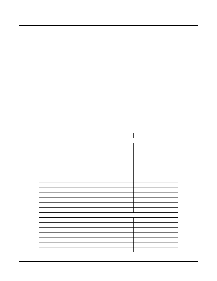
Table 2-7. Supported Input Standards
Input Standard
VREF (Nom.)
VCCIO
1 (Nom.)
Single Ended Interfaces
LVTTL
—
LVCMOS33
2
——
LVCMOS25
2
——
LVCMOS18
—
1.8
LVCMOS15
—
1.5
LVCMOS12
2
——
PCI
—
3.3
HSTL18 Class I, II
0.9
—
HSTL18 Class III
1.08
—
HSTL15 Class I
0.75
—
HSTL15 Class III
0.9
—
SSTL3 Class I, II
1.5
—
SSTL2 Class I, II
1.25
—
SSTL18 Class I
0.9
—
Differential Interfaces
Differential SSTL18 Class I
—
Differential SSTL2 Class I, II
—
Differential SSTL3 Class I, II
—
Differential HSTL15 Class I, III
—
Differential HSTL18 Class I, II, III
—
LVDS, LVPECL
—
BLVDS
—
1. When not specified VCCIO can be set anywhere in the valid operating range.
2. JTAG inputs do not have a fixed threshold option and always follow VCCJ.
相關(guān)PDF資料 |
PDF描述 |
|---|---|
| LFZ3508VXX | GENERAL PURPOSE INDUCTOR |
| LFZ2805HXX | GENERAL PURPOSE INDUCTOR |
| LF02004VTX | GENERAL PURPOSE INDUCTOR |
| LG3341-NE7501 | T-1 SINGLE COLOR LED, GREEN, 3 mm |
| LG3341-KNE9117 | T-1 SINGLE COLOR LED, GREEN, 3 mm |
相關(guān)代理商/技術(shù)參數(shù) |
參數(shù)描述 |
|---|---|
| LFXP15C-4FN256I | 功能描述:FPGA - 現(xiàn)場可編程門陣列 15.4K LUTs 188 IO 1. 8/2.5/3.3V-4 Spd I RoHS:否 制造商:Altera Corporation 系列:Cyclone V E 柵極數(shù)量: 邏輯塊數(shù)量:943 內(nèi)嵌式塊RAM - EBR:1956 kbit 輸入/輸出端數(shù)量:128 最大工作頻率:800 MHz 工作電源電壓:1.1 V 最大工作溫度:+ 70 C 安裝風(fēng)格:SMD/SMT 封裝 / 箱體:FBGA-256 |
| LFXP15C-4FN388C | 功能描述:FPGA - 現(xiàn)場可編程門陣列 15.4K LUTs 268 IO 1. 8/2.5/3.3V -4 Spd RoHS:否 制造商:Altera Corporation 系列:Cyclone V E 柵極數(shù)量: 邏輯塊數(shù)量:943 內(nèi)嵌式塊RAM - EBR:1956 kbit 輸入/輸出端數(shù)量:128 最大工作頻率:800 MHz 工作電源電壓:1.1 V 最大工作溫度:+ 70 C 安裝風(fēng)格:SMD/SMT 封裝 / 箱體:FBGA-256 |
| LFXP15C-4FN388I | 功能描述:FPGA - 現(xiàn)場可編程門陣列 15.4K LUTs 268 IO 1. 8/2.5/3.3V-4 Spd I RoHS:否 制造商:Altera Corporation 系列:Cyclone V E 柵極數(shù)量: 邏輯塊數(shù)量:943 內(nèi)嵌式塊RAM - EBR:1956 kbit 輸入/輸出端數(shù)量:128 最大工作頻率:800 MHz 工作電源電壓:1.1 V 最大工作溫度:+ 70 C 安裝風(fēng)格:SMD/SMT 封裝 / 箱體:FBGA-256 |
| LFXP15C-4FN484C | 功能描述:FPGA - 現(xiàn)場可編程門陣列 15.4K LUTs 1.8/2.5/3 .3V -4 Spd RoHS:否 制造商:Altera Corporation 系列:Cyclone V E 柵極數(shù)量: 邏輯塊數(shù)量:943 內(nèi)嵌式塊RAM - EBR:1956 kbit 輸入/輸出端數(shù)量:128 最大工作頻率:800 MHz 工作電源電壓:1.1 V 最大工作溫度:+ 70 C 安裝風(fēng)格:SMD/SMT 封裝 / 箱體:FBGA-256 |
| LFXP15C-4FN484I | 功能描述:FPGA - 現(xiàn)場可編程門陣列 15.4K LUTs 1.8/2.5/3 .3V-4 Spd I RoHS:否 制造商:Altera Corporation 系列:Cyclone V E 柵極數(shù)量: 邏輯塊數(shù)量:943 內(nèi)嵌式塊RAM - EBR:1956 kbit 輸入/輸出端數(shù)量:128 最大工作頻率:800 MHz 工作電源電壓:1.1 V 最大工作溫度:+ 70 C 安裝風(fēng)格:SMD/SMT 封裝 / 箱體:FBGA-256 |
發(fā)布緊急采購,3分鐘左右您將得到回復(fù)。