- 您現(xiàn)在的位置:買賣IC網(wǎng) > PDF目錄299403 > LFXP15C-4FN256C (LATTICE SEMICONDUCTOR CORP) PDF資料下載
參數(shù)資料
| 型號: | LFXP15C-4FN256C |
| 廠商: | LATTICE SEMICONDUCTOR CORP |
| 元件分類: | FPGA |
| 中文描述: | FPGA, 1932 CLBS, PBGA256 |
| 封裝: | 17 X 17 MM, LEAD FREE, FPBGA-256 |
| 文件頁數(shù): | 40/130頁 |
| 文件大?。?/td> | 1312K |
| 代理商: | LFXP15C-4FN256C |
第1頁第2頁第3頁第4頁第5頁第6頁第7頁第8頁第9頁第10頁第11頁第12頁第13頁第14頁第15頁第16頁第17頁第18頁第19頁第20頁第21頁第22頁第23頁第24頁第25頁第26頁第27頁第28頁第29頁第30頁第31頁第32頁第33頁第34頁第35頁第36頁第37頁第38頁第39頁當(dāng)前第40頁第41頁第42頁第43頁第44頁第45頁第46頁第47頁第48頁第49頁第50頁第51頁第52頁第53頁第54頁第55頁第56頁第57頁第58頁第59頁第60頁第61頁第62頁第63頁第64頁第65頁第66頁第67頁第68頁第69頁第70頁第71頁第72頁第73頁第74頁第75頁第76頁第77頁第78頁第79頁第80頁第81頁第82頁第83頁第84頁第85頁第86頁第87頁第88頁第89頁第90頁第91頁第92頁第93頁第94頁第95頁第96頁第97頁第98頁第99頁第100頁第101頁第102頁第103頁第104頁第105頁第106頁第107頁第108頁第109頁第110頁第111頁第112頁第113頁第114頁第115頁第116頁第117頁第118頁第119頁第120頁第121頁第122頁第123頁第124頁第125頁第126頁第127頁第128頁第129頁第130頁
2-14
Architecture
Lattice Semiconductor
LatticeXP Family Data Sheet
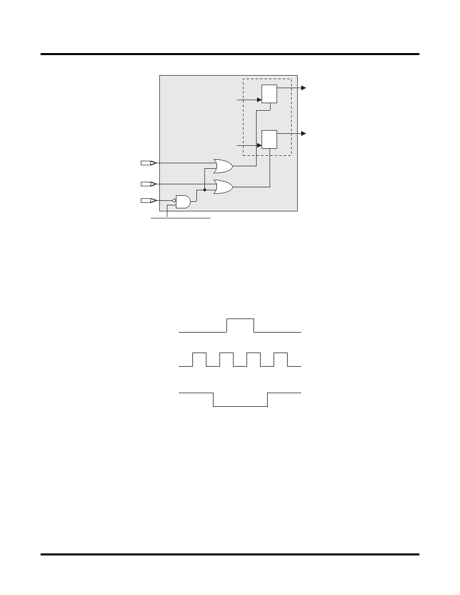
Figure 2-15. Memory Core Reset
For further information on sysMEM EBR block, see the details of additional technical documentation at the end of
this data sheet.
EBR Asynchronous Reset
EBR asynchronous reset or GSR (if used) can only be applied if all clock enables are low for a clock cycle before the
reset is applied and released a clock cycle after the reset is released, as shown in Figure 2-16. The GSR input to the
EBR is always asynchronous.
Figure 2-16. EBR Asynchronous Reset (Including GSR) Timing Diagram
If all clock enables remain enabled, the EBR asynchronous reset or GSR may only be applied and released after
the EBR read and write clock inputs are in a steady state condition for a minimum of 1/fMAX (EBR clock). The reset
release must adhere to the EBR synchronous reset setup time before the next active read or write clock edge.
If an EBR is pre-loaded during configuration, the GSR input must be disabled or the release of the GSR during
device Wake Up must occur before the release of the device I/Os becoming active.
These instructions apply to all EBR RAM and ROM implementations.
Note that there are no reset restrictions if the EBR synchronous reset is used and the EBR GSR input is disabled.
Programmable I/O Cells (PICs)
Each PIC contains two PIOs connected to their respective sysIO Buffers which are then connected to the PADs as
shown in Figure 2-17. The PIO Block supplies the output data (DO) and the Tri-state control signal (TO) to sysIO
buffer, and receives input from the buffer.
Q
SET
D
LCLR
Output Data
Latches
Memory Core
Port A[17:0]
Q
SET
D
Port B[17:0]
RSTB
GSRN
Programmable Disable
RSTA
LCLR
Reset
Clock
Enable
相關(guān)PDF資料 |
PDF描述 |
|---|---|
| LFZ3508VXX | GENERAL PURPOSE INDUCTOR |
| LFZ2805HXX | GENERAL PURPOSE INDUCTOR |
| LF02004VTX | GENERAL PURPOSE INDUCTOR |
| LG3341-NE7501 | T-1 SINGLE COLOR LED, GREEN, 3 mm |
| LG3341-KNE9117 | T-1 SINGLE COLOR LED, GREEN, 3 mm |
相關(guān)代理商/技術(shù)參數(shù) |
參數(shù)描述 |
|---|---|
| LFXP15C-4FN256I | 功能描述:FPGA - 現(xiàn)場可編程門陣列 15.4K LUTs 188 IO 1. 8/2.5/3.3V-4 Spd I RoHS:否 制造商:Altera Corporation 系列:Cyclone V E 柵極數(shù)量: 邏輯塊數(shù)量:943 內(nèi)嵌式塊RAM - EBR:1956 kbit 輸入/輸出端數(shù)量:128 最大工作頻率:800 MHz 工作電源電壓:1.1 V 最大工作溫度:+ 70 C 安裝風(fēng)格:SMD/SMT 封裝 / 箱體:FBGA-256 |
| LFXP15C-4FN388C | 功能描述:FPGA - 現(xiàn)場可編程門陣列 15.4K LUTs 268 IO 1. 8/2.5/3.3V -4 Spd RoHS:否 制造商:Altera Corporation 系列:Cyclone V E 柵極數(shù)量: 邏輯塊數(shù)量:943 內(nèi)嵌式塊RAM - EBR:1956 kbit 輸入/輸出端數(shù)量:128 最大工作頻率:800 MHz 工作電源電壓:1.1 V 最大工作溫度:+ 70 C 安裝風(fēng)格:SMD/SMT 封裝 / 箱體:FBGA-256 |
| LFXP15C-4FN388I | 功能描述:FPGA - 現(xiàn)場可編程門陣列 15.4K LUTs 268 IO 1. 8/2.5/3.3V-4 Spd I RoHS:否 制造商:Altera Corporation 系列:Cyclone V E 柵極數(shù)量: 邏輯塊數(shù)量:943 內(nèi)嵌式塊RAM - EBR:1956 kbit 輸入/輸出端數(shù)量:128 最大工作頻率:800 MHz 工作電源電壓:1.1 V 最大工作溫度:+ 70 C 安裝風(fēng)格:SMD/SMT 封裝 / 箱體:FBGA-256 |
| LFXP15C-4FN484C | 功能描述:FPGA - 現(xiàn)場可編程門陣列 15.4K LUTs 1.8/2.5/3 .3V -4 Spd RoHS:否 制造商:Altera Corporation 系列:Cyclone V E 柵極數(shù)量: 邏輯塊數(shù)量:943 內(nèi)嵌式塊RAM - EBR:1956 kbit 輸入/輸出端數(shù)量:128 最大工作頻率:800 MHz 工作電源電壓:1.1 V 最大工作溫度:+ 70 C 安裝風(fēng)格:SMD/SMT 封裝 / 箱體:FBGA-256 |
| LFXP15C-4FN484I | 功能描述:FPGA - 現(xiàn)場可編程門陣列 15.4K LUTs 1.8/2.5/3 .3V-4 Spd I RoHS:否 制造商:Altera Corporation 系列:Cyclone V E 柵極數(shù)量: 邏輯塊數(shù)量:943 內(nèi)嵌式塊RAM - EBR:1956 kbit 輸入/輸出端數(shù)量:128 最大工作頻率:800 MHz 工作電源電壓:1.1 V 最大工作溫度:+ 70 C 安裝風(fēng)格:SMD/SMT 封裝 / 箱體:FBGA-256 |
發(fā)布緊急采購,3分鐘左右您將得到回復(fù)。