- 您現(xiàn)在的位置:買賣IC網(wǎng) > PDF目錄358757 > LC6529F (Sanyo Electric Co.,Ltd.) 4-Bit Microcomputer for Small-Scale Control Applications PDF資料下載
參數(shù)資料
| 型號: | LC6529F |
| 廠商: | Sanyo Electric Co.,Ltd. |
| 英文描述: | 4-Bit Microcomputer for Small-Scale Control Applications |
| 中文描述: | 4小位微機(jī)控制應(yīng)用規(guī)模 |
| 文件頁數(shù): | 15/39頁 |
| 文件大小: | 525K |
| 代理商: | LC6529F |
第1頁第2頁第3頁第4頁第5頁第6頁第7頁第8頁第9頁第10頁第11頁第12頁第13頁第14頁當(dāng)前第15頁第16頁第17頁第18頁第19頁第20頁第21頁第22頁第23頁第24頁第25頁第26頁第27頁第28頁第29頁第30頁第31頁第32頁第33頁第34頁第35頁第36頁第37頁第38頁第39頁
LC6529F
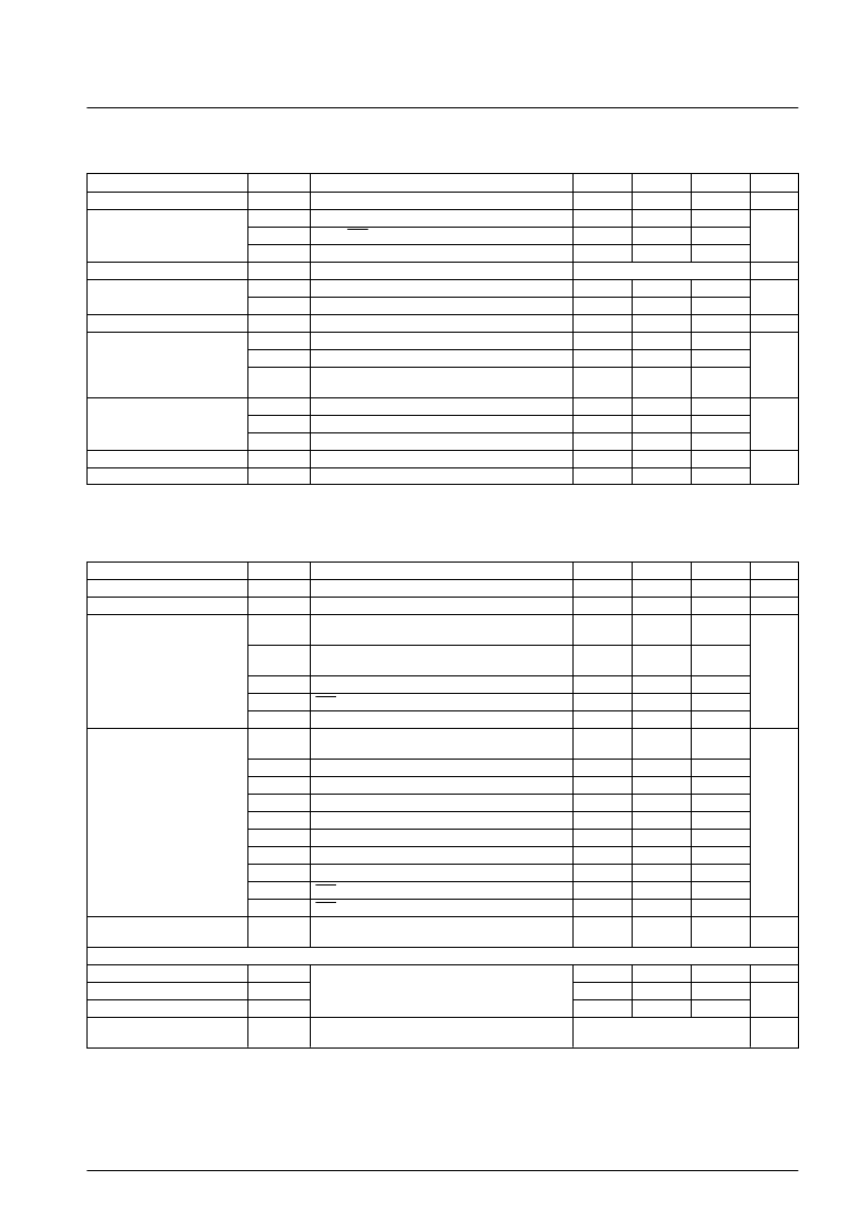
Absolute Maximum Ratings
at Ta = 25°C, V
SS
= 0 V
Note: 1. When the oscillator circuit in Figure 3 and the guaranteed constant are used, this is guaranteed over the full amplitude.
2. Averaged over 100-ms interval.
Allowable Operating Ranges
at Ta = –40 to +85°C, V
SS
= 0 V, V
DD
= 3.0 to 6.0 V
Note:
*
Maintain the power supply voltage at V
DD
until the HALT instruction has completed execution, placing the chip in the standby mode. Block
chattering from entering PA3 during the HALT instruction execution cycle.
No. 5117-15/39
LC6529N, LC6529F, LC6529L
Parameter
Symbol
Conditions
min
typ
max
Unit
Maximum supply voltage
V
DD
max
V
I
1
V
I
2
V
I
3
V
O
V
IO
1
V
IO
2
I
OP
I
OA
Σ
I
OA
1
V
DD
OSC1
*
1
–0.3
+7.0
V
–0.3
V
DD
+ 0.3
V
DD
+ 0.3
V
DD
+ 0.3
Input voltage
TEST, RES
–0.3
V
Port E (PE) configuration
–0.3
Output voltage
OSC2
Voltages up to that generated allowed.
V
I/O voltages
Open-drain (OD) configuration
–0.3
+15
V
Pull-up (PU) resistor configuration
–0.3
V
DD
+ 0.3
Peak output current
PA, PC, PD
–2
+20
mA
PA, PC, PD: Average for pin over 100-ms interval
PA: Total current for pins PA0 to PA3
*
2
–2
+20
Average output current
–6
+40
mA
Σ
I
OA
2
PC, PD: Total current for pins PC0 to PC3 and
PD0 to PD3
*
2
–14
+90
Pd max1
Ta = –40 to +85°C (DIP24S)
360
Allowable power dissipation
Pd max2
Ta = –40 to +85°C (SSOP24)
165
mW
Pd max3
Ta = –40 to +85°C (MFP30S)
150
Operating temperature
Topr
–40
+85
°C
Storage temperature
Tstg
–55
+125
Parameter
Symbol
Conditions
min
typ
max
Unit
Supply voltage
V
DD
V
ST
V
DD
V
DD
: Preserves contents of RAM and registers
*
.
Open-drain (OD) configuration: With output N-channel
transistor off
3.0
6.0
V
Standby voltage
1.8
6.0
V
V
IH
1
0.7 V
DD
13.5
V
IH
2
Pull-up (PU) resistor configuration: With output
N-channel transistor off
0.7 V
DD
V
DD
Input high level voltage
V
V
IH
3
V
IH
4
V
IH
5
PE: Using port E configuration
0.7 V
DD
0.8 V
DD
0.8 V
DD
V
DD
V
DD
V
DD
RES: V
DD
= 1.8 to 6 V
OSC1: Using external clock option
V
IL
1
PA, PC, PD: With output N-channel transistor off,
V
DD
= 4 to 6 V
PA, PC, PD: With output N-channel transistor off
V
SS
0.3 V
DD
V
IL
2
V
IL
3
V
IL
4
V
IL
5
V
IL
6
V
IL
7
V
IL
8
V
IL
9
V
IL
10
fop
(Tcyc)
V
SS
V
SS
V
SS
V
SS
V
SS
V
SS
V
SS
V
SS
V
SS
200
(20)
0.25 V
DD
0.3 V
DD
0.25 V
DD
0.25 V
DD
0.2 V
DD
0.3 V
DD
0.25 V
DD
0.25 V
DD
0.2 V
DD
4330
(0.92)
PE: Using port E configuration, V
DD
= 4 to 6 V
PE: Using port E configuration
Input low level voltage
OSC1: Using external clock option, V
DD
= 4 to 6 V
OSC1: Using external clock option
V
TEST: V
DD
= 4 to 6 V
TEST
RES: V
DD
= 4 to 6 V
RES
Operating frequency
(cycle time)
kHz
(μs)
[External clock conditions]
Frequency
text
200
4330
kHz
Pulse width
textH, textL
OSC1: Figure 1
69
ns
Rise/fall times
textR, textF
50
Oscillator guaranteed constants
Ceramic oscillator
Figure 2
See Table 1.
相關(guān)PDF資料 |
PDF描述 |
|---|---|
| LC6538D | SINGLE-CHIP 4-BIT MICROCOMPUTER FOR LARGE-SCALE CONTROL-ORIENTED APPLICATIONS |
| LC65404A | 4-BIT Single Chip MICROCOMPUTER FOR CONTROL APPLICATIONS |
| LC6543F | Single-chip 4-bit Microcomputer for Small-scale Control-oriented Applications(用于小規(guī)模控制定位應(yīng)用的單片4位微控制器) |
| LC6546C | RESISTOR-20K,1/10W,1% MFILM |
| LC6554D | 4K-Byte ROM-Contained Single-chip 4-Bit Microcomputer with FLT,LED Drivers(4K字節(jié)ROM的單片4位微控制器帶FLT,LED驅(qū)動器) |
相關(guān)代理商/技術(shù)參數(shù) |
參數(shù)描述 |
|---|---|
| LC6529H | 制造商:未知廠家 制造商全稱:未知廠家 功能描述: |
| LC6529L | 制造商:SANYO 制造商全稱:Sanyo Semicon Device 功能描述:One-Time Programmable 4-Bit Single-Chip Microcontroller |
| LC6529N | 制造商:SANYO 制造商全稱:Sanyo Semicon Device 功能描述:One-Time Programmable 4-Bit Single-Chip Microcontroller |
| LC6530C | 制造商:未知廠家 制造商全稱:未知廠家 功能描述:Microcontroller |
| LC6532C | 制造商:未知廠家 制造商全稱:未知廠家 功能描述:Microcontroller |
發(fā)布緊急采購,3分鐘左右您將得到回復(fù)。