- 您現在的位置:買賣IC網 > PDF目錄223993 > HY5V52EMP-H (HYNIX SEMICONDUCTOR INC) 8M X 32 SYNCHRONOUS DRAM, 5.4 ns, PBGA90 PDF資料下載
參數資料
| 型號: | HY5V52EMP-H |
| 廠商: | HYNIX SEMICONDUCTOR INC |
| 元件分類: | DRAM |
| 英文描述: | 8M X 32 SYNCHRONOUS DRAM, 5.4 ns, PBGA90 |
| 封裝: | 8 X 13 MM, 1.20 MM HEIGHT, 0.80 MM PITCH, LEAD FREE, FBGA-90 |
| 文件頁數: | 10/14頁 |
| 文件大小: | 172K |
| 代理商: | HY5V52EMP-H |
Rev. 1.0 / Nov. 2005
5
1
Synchronous DRAM Memory 256Mbit (8Mx16bit *2stack)
HY5V52E(L)M(P) Series
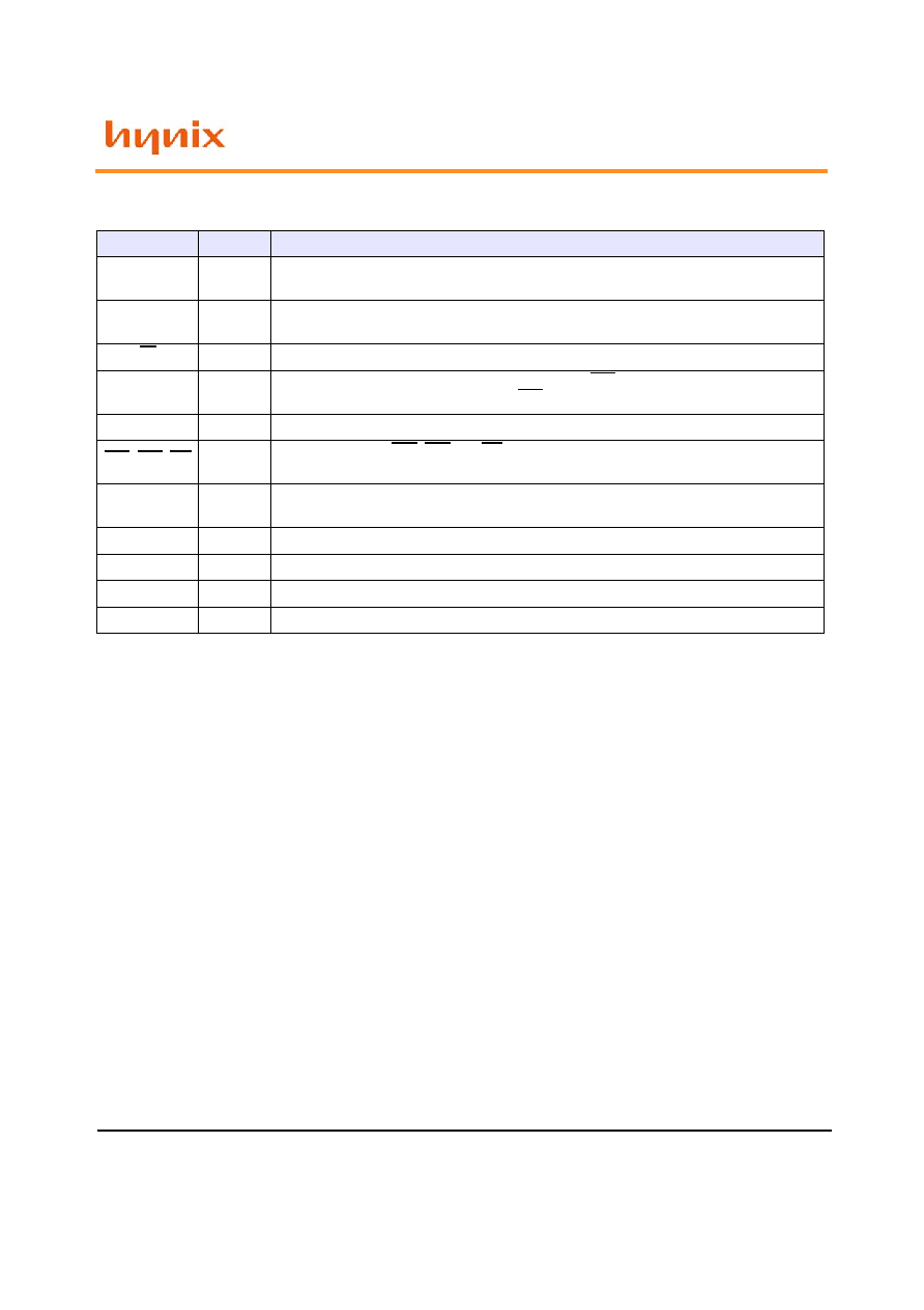
BALL DESCRIPTIONS
SYMBOL
TYPE
DESCRIPTION
CLK
INPUT
Clock: The system clock input. All other inputs are registered to the SDRAM on the rising
edge of CLK
CKE
INPUT
Clock Enable: Controls internal clock signal and when deactivated, the SDRAM will be one
of the states among power down, suspend or self refresh
CS
INPUT
Chip Select: Enables or disables all inputs except CLK, CKE and DQM
BA0, BA1
INPUT
Bank Address: Selects bank to be activated during RAS activity
Selects bank to be read/written during CAS activity
A0 ~ A11
INPUT
Row Address: RA0 ~ RA11, Column Address: CA0 ~ CA8, Auto-precharge flag: A10
RAS, CAS, WE
INPUT
Command Inputs: RAS, CAS and WE define the operation
Refer function truth table for details
DQM0 ~
DQM3
I/O
Data Mask: Controls output buffers in read mode and masks input data in write mode
DQ0 ~ DQ31
I/O
Data Input / Output: Multiplexed data input / output pin
VDD / VSS
SUPPLY
Power supply
VDDQ / VSSQ
SUPPLY
I/O Power supply
NC
-
No connection : These pads should be left unconnected
相關PDF資料 |
PDF描述 |
|---|---|
| HY5V56BSF-8 | 16M X 16 SYNCHRONOUS DRAM, 6 ns, PBGA54 |
| HY62256ALLR1-70 | x8 SRAM |
| HY62256ALLR1-85 | x8 SRAM |
| HY62256ALLT1-10 | x8 SRAM |
| HY62256ALLT1-55 | x8 SRAM |
相關代理商/技術參數 |
參數描述 |
|---|---|
| HY5V52F | 制造商:HYNIX 制造商全稱:Hynix Semiconductor 功能描述:4Banks x 2M x 32bits Synchronous DRAM |
| HY5V52F-H | 制造商:HYNIX 制造商全稱:Hynix Semiconductor 功能描述:4Banks x 2M x 32bits Synchronous DRAM |
| HY5V52F-P | 制造商:HYNIX 制造商全稱:Hynix Semiconductor 功能描述:4Banks x 2M x 32bits Synchronous DRAM |
| HY5V52FP-H | 制造商:HYNIX 制造商全稱:Hynix Semiconductor 功能描述:4Banks x 2M x 32bits Synchronous DRAM |
| HY5V52FP-P | 制造商:HYNIX 制造商全稱:Hynix Semiconductor 功能描述:4Banks x 2M x 32bits Synchronous DRAM |
發(fā)布緊急采購,3分鐘左右您將得到回復。