- 您現(xiàn)在的位置:買賣IC網(wǎng) > PDF目錄223992 > HY27US081G1MTPMP (HYNIX SEMICONDUCTOR INC) 128M X 8 FLASH 2.7V PROM, 45 ns, PDSO48 PDF資料下載
參數(shù)資料
| 型號: | HY27US081G1MTPMP |
| 廠商: | HYNIX SEMICONDUCTOR INC |
| 元件分類: | PROM |
| 英文描述: | 128M X 8 FLASH 2.7V PROM, 45 ns, PDSO48 |
| 封裝: | 12 X 20 MM, 1.20 MM HEIGHT, LEAD FREE, TSOP1-48 |
| 文件頁數(shù): | 28/39頁 |
| 文件大小: | 312K |
| 代理商: | HY27US081G1MTPMP |
第1頁第2頁第3頁第4頁第5頁第6頁第7頁第8頁第9頁第10頁第11頁第12頁第13頁第14頁第15頁第16頁第17頁第18頁第19頁第20頁第21頁第22頁第23頁第24頁第25頁第26頁第27頁當前第28頁第29頁第30頁第31頁第32頁第33頁第34頁第35頁第36頁第37頁第38頁第39頁
Rev 0.2 / May. 2007
34
Preliminary
HY27US(08/16)1G1M Series
1Gbit (128Mx8bit / 64Mx16bit) NAND Flash
Bad Block Management
Devices with Bad Blocks have the same quality level and the same AC and DC characteristics as devices where all the blocks are valid.
A Bad Block does not affect the performance of valid blocks because it is isolated from the bit line and common source line by a
select transistor. The devices are supplied with all the locations inside valid blocks erased(FFh/FFFFh).
The Bad Block Information is written prior to shipping. Any block where the 6th Byte/ 1st Word in the spare area of the 1st or 2nd
page (if the 1st page is Bad) does not contain FFh/FFFFh is a Bad Block. The Bad Block Information must be read before any erase is
attempted as the Bad Block Information may be erased. For the system to be able to recognize the Bad Blocks based on the original
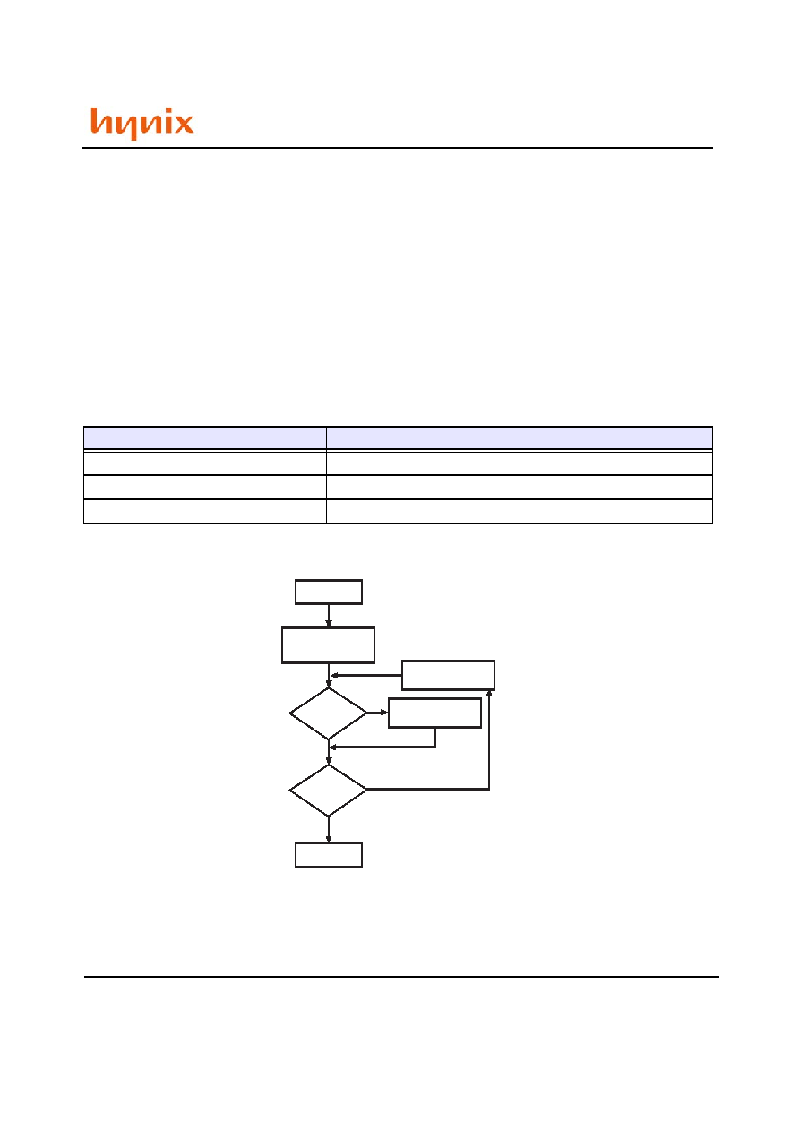
information it is recommended to create a Bad Block table following the flowchart shown in Figure 26. The 1st block, which is placed
on 00h block address is guaranteed to be a valid block.
Block Replacement
Over the lifetime of the device additional Bad Blocks may develop. In this case the block has to be replaced by copying the data to a
valid block. These additional Bad Blocks can be identified as attempts to program or erase them will give errors in the Status Regis-
ter.
As the failure of a page program operation does not affect the data in other pages in the same block, the block can be replaced by
re-programming the current data and copying the rest of the replaced block to an available valid block.
The Copy Back Program command can be used to copy the data to a valid block.
See the “Copy Back Program” section for more details.
Refer to Table 16 for the recommended procedure to follow if an error occurs during an operation.
Operation
Recommended Procedure
Erase
Block Replacement
Program
Block Replacement or ECC (with 4bit/528byte)
Read
ECC (with 4bit/528byte)
Table 16: Block Failure
Figure 26: Bad Block Management Flowchart
相關(guān)PDF資料 |
PDF描述 |
|---|---|
| HY5116100BJ-70 | 16M X 1 FAST PAGE DRAM, 70 ns, PDSO24 |
| HY5116804CSLT-80 | 2M X 8 EDO DRAM, 80 ns, PDSO28 |
| HY514400ALT-60 | 1M X 4 FAST PAGE DRAM, 60 ns, PDSO20 |
| HY51VS65173HGLT-5 | 4M X 16 EDO DRAM, 50 ns, PDSO50 |
| HY57V283220LT-7I | 4M X 32 SYNCHRONOUS DRAM, 5.5 ns, PDSO86 |
相關(guān)代理商/技術(shù)參數(shù) |
參數(shù)描述 |
|---|---|
| HY27US08281A | 制造商:HYNIX 制造商全稱:Hynix Semiconductor 功能描述:128Mbit (16Mx8bit / 8Mx16bit) NAND Flash Memory |
| HY27US08282A | 制造商:HYNIX 制造商全稱:Hynix Semiconductor 功能描述:128Mbit (16Mx8bit / 8Mx16bit) NAND Flash Memory |
| HY27US08561A | 制造商:HYNIX 制造商全稱:Hynix Semiconductor 功能描述:256Mbit (32Mx8bit / 16Mx16bit) NAND Flash |
| HY27US08561A-T (P) | 制造商:SK Hynix Inc 功能描述: |
| HY27US08561M | 制造商:HYNIX 制造商全稱:Hynix Semiconductor 功能描述:256Mbit (32Mx8bit / 16Mx16bit) NAND Flash |
發(fā)布緊急采購,3分鐘左右您將得到回復。