- 您現(xiàn)在的位置:買(mǎi)賣(mài)IC網(wǎng) > PDF目錄370667 > HPMX-7201 Upconverter(上變頻器) PDF資料下載
參數(shù)資料
| 型號(hào): | HPMX-7201 |
| 英文描述: | Upconverter(上變頻器) |
| 中文描述: | 變頻器(上變頻器) |
| 文件頁(yè)數(shù): | 15/19頁(yè) |
| 文件大?。?/td> | 163K |
| 代理商: | HPMX-7201 |
第1頁(yè)第2頁(yè)第3頁(yè)第4頁(yè)第5頁(yè)第6頁(yè)第7頁(yè)第8頁(yè)第9頁(yè)第10頁(yè)第11頁(yè)第12頁(yè)第13頁(yè)第14頁(yè)當(dāng)前第15頁(yè)第16頁(yè)第17頁(yè)第18頁(yè)第19頁(yè)
15
5.4 dBm – urban) is significantly
lower than the maximum. (Note:
the average transmit power is not
at the peak of the distribution
functions shown in Figure 34
because of the logarithmic scale
on the x-axis).
Current consumption in the
transmit chain at maximum
output is many times considered
the
only
critical figure of merit
for selecting the RF components
to be used in a handset design.
Current consumption at maxi-
mum output power is of course
still important, for both RF and
thermal design reasons. For
example, an additional incentive
for keeping the current consump-
tion maximum output power as
low as possible, is that the
statistical profiles will vary from
user to user depending on usage
patterns and conditions. In other
words, although the statistical
profiles published by the CDG
obey the laws of large numbers,
the statistical profile for an
individual user may differ
significantly.
Having said that
,
the real figure of
merit for CDMA mobile phone
should be the
statistical-average
current
consumption
, Icc-
μ
which is the current consumption
integrated over the user’s statisti-
cal profile. In fact, the CDG’s talk-
time method of measurement
consists of continuously sweep-
ing the output power of the
mobile from –50 to +23 dBm
according to the statistical
profiles shown in Figure 34, to
arrive at an industry-standard
definition of talk-time (CDG Stage
4 system performance tests).
If the RF components have a
fixed bias, then the current
consumption at maximum output
power is the same as the
statistical-average current
consumption. This is often the
case with the baseband and first
IF stages of many radio designs,
but in the higher power stages,
particularly the PA driver and the
PA itself the supply current is a
strong function of output power.
However, if the RF components
use adaptive-bias techniques such
that the current consumption
decreases with the output power,
then the maximum and statistical-
average current consumption can
be set independently, optimizing
each one as needed. The current
consumption at maximum output
power is designed to deliver the
required linearity, while the
statistical-average current
consumption is designed to
maximize talk-time. Figure 34
illustrates the fact that the mobile
spends – statistically – little time
at the maximum output power,
and therefore the current con-
sumption at that point has only a
minor influence on the statistical-
average current and, by exten-
sion, on talk-time.
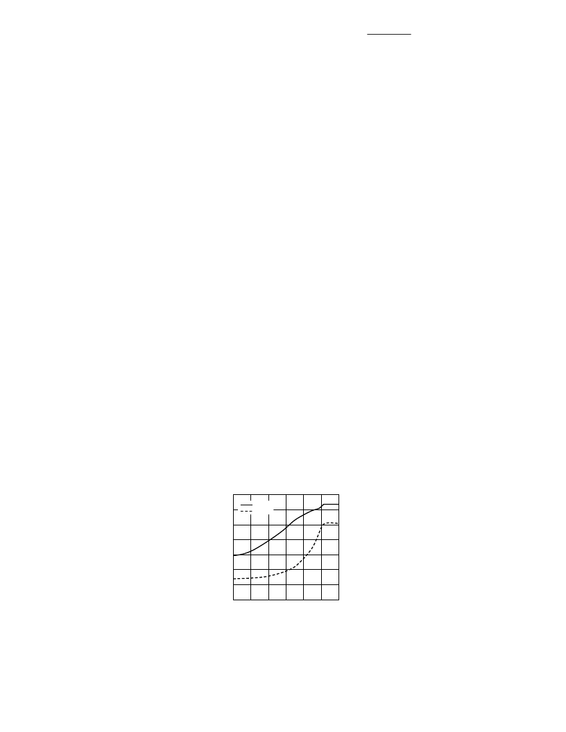
RfTxAgc VOLTAGE (V)
G
I
0
30
20
10
0
-10
-20
-30
-40
140
120
100
80
60
40
20
0
3
1
0.5
2
2.5
1.5
Gain
Icc-bat
Figure 35: HPMX-7201 RF VGA Gain
and Supply Current Consumption vs.
RfTxAgc Voltage.
Figure 35 illustrates the effect of
using adaptive bias techniques in
the RF VGA of the HPMX-7201.
The plot shows the measured
gain and current consumption vs.
the gain control voltage, RfTxAgc,
for one of the CDMA outputs. As
the gain is reduced, and hence the
output power, the current con-
sumption decreases while still
maintaining an adequate ACPR.
Note that the current plotted is
only the VGA current, the mixer
current is not included.
Figure 36 shows the
total
current
consumption for the HPMX-7201
versus output power
for a
constant ACPR of -55 dBc/
30 KHz
(this ACPR was selected
arbitrarily; similar plots can be
produced for other values). The
plot was generated by adjusting
the input power and the gain
control voltage to achieve the
ACPR= –55 dBc at the lowest
possible current consumption, for
each output power. The HPMX-
7201 can deliver up to +14 dBm of
power. The lower trace on the
plot show how the total current
varies versus output power if the
gain control voltage is adjusted
continuously. The next (middle)
trace illustrates the performance
of the device if the gain control
voltage adjustment is limited to 3
discrete states, rather than a
continuum. This method simpli-
fies the operation of the part, at
the expense of a higher statisti-
cal-average current consumption.
The upper trace illustrates the
performance if the gain control
voltage adjustment is further
limited to only 2 discrete states.
相關(guān)PDF資料 |
PDF描述 |
|---|---|
| HPND-0002 | Small Signal RF PIN Diode Chips for Hybrid Integrated Circuits(小信號(hào)射頻PIN二極管晶片(用于混合集成電路)) |
| HPND-0001 | Small Signal RF PIN Diode Chips for Hybrid Integrated Circuits(小信號(hào)射頻PIN二極管晶片(用于混合集成電路)) |
| HPND-4005 | Beam Lead PIN Diode(束引線(xiàn)PIN二極管) |
| HPND-4018 | Beam Lead PIN Diodes for Phased Arrays and Switches(束引線(xiàn)PIN二極管(用于相位陣列和開(kāi)關(guān))) |
| HPND-4028 | Beam Lead PIN Diodes for Phased Arrays and Switches(束引線(xiàn)PIN二極管(用于相位陣列和開(kāi)關(guān))) |
相關(guān)代理商/技術(shù)參數(shù) |
參數(shù)描述 |
|---|---|
| HPMX-7202 | 制造商:未知廠(chǎng)家 制造商全稱(chēng):未知廠(chǎng)家 功能描述:DBTM Upconverter |
| HPN | 功能描述:熔絲座 BUSS FUSEHOLDER RoHS:否 制造商:Littelfuse 產(chǎn)品: 電流額定值:30 A 電壓額定值:1000 VDC 極數(shù):1 系列: 安裝風(fēng)格:DIN Rail 端接類(lèi)型: 軸類(lèi)型: 工作溫度范圍: |
| HPN-0689B | 制造商:JST Manufacturing 功能描述:Information pending |
| HPN-0689C | 制造商:JST Manufacturing 功能描述:Information pending |
| HPN2222A | 制造商:HSMC 制造商全稱(chēng):HSMC 功能描述:NPN EPITAXIAL PLANAR TRANSISTOR |
發(fā)布緊急采購(gòu),3分鐘左右您將得到回復(fù)。