- 您現(xiàn)在的位置:買(mǎi)賣(mài)IC網(wǎng) > PDF目錄4482 > EP1K50FI256-2N (Altera)IC ACEX 1K FPGA 50K 256-FBGA PDF資料下載
參數(shù)資料
| 型號(hào): | EP1K50FI256-2N |
| 廠商: | Altera |
| 文件頁(yè)數(shù): | 49/86頁(yè) |
| 文件大?。?/td> | 0K |
| 描述: | IC ACEX 1K FPGA 50K 256-FBGA |
| 產(chǎn)品培訓(xùn)模塊: | Three Reasons to Use FPGA's in Industrial Designs |
| 標(biāo)準(zhǔn)包裝: | 90 |
| 系列: | ACEX-1K® |
| LAB/CLB數(shù): | 360 |
| 邏輯元件/單元數(shù): | 2880 |
| RAM 位總計(jì): | 40960 |
| 輸入/輸出數(shù): | 186 |
| 門(mén)數(shù): | 199000 |
| 電源電壓: | 2.375 V ~ 2.625 V |
| 安裝類(lèi)型: | 表面貼裝 |
| 工作溫度: | -40°C ~ 85°C |
| 封裝/外殼: | 256-BGA |
| 供應(yīng)商設(shè)備封裝: | 256-FBGA(17x17) |
第1頁(yè)第2頁(yè)第3頁(yè)第4頁(yè)第5頁(yè)第6頁(yè)第7頁(yè)第8頁(yè)第9頁(yè)第10頁(yè)第11頁(yè)第12頁(yè)第13頁(yè)第14頁(yè)第15頁(yè)第16頁(yè)第17頁(yè)第18頁(yè)第19頁(yè)第20頁(yè)第21頁(yè)第22頁(yè)第23頁(yè)第24頁(yè)第25頁(yè)第26頁(yè)第27頁(yè)第28頁(yè)第29頁(yè)第30頁(yè)第31頁(yè)第32頁(yè)第33頁(yè)第34頁(yè)第35頁(yè)第36頁(yè)第37頁(yè)第38頁(yè)第39頁(yè)第40頁(yè)第41頁(yè)第42頁(yè)第43頁(yè)第44頁(yè)第45頁(yè)第46頁(yè)第47頁(yè)第48頁(yè)當(dāng)前第49頁(yè)第50頁(yè)第51頁(yè)第52頁(yè)第53頁(yè)第54頁(yè)第55頁(yè)第56頁(yè)第57頁(yè)第58頁(yè)第59頁(yè)第60頁(yè)第61頁(yè)第62頁(yè)第63頁(yè)第64頁(yè)第65頁(yè)第66頁(yè)第67頁(yè)第68頁(yè)第69頁(yè)第70頁(yè)第71頁(yè)第72頁(yè)第73頁(yè)第74頁(yè)第75頁(yè)第76頁(yè)第77頁(yè)第78頁(yè)第79頁(yè)第80頁(yè)第81頁(yè)第82頁(yè)第83頁(yè)第84頁(yè)第85頁(yè)第86頁(yè)
Altera Corporation
53
ACEX 1K Programmable Logic Device Family Data Sheet
D
e
ve
lo
pm
e
n
t
13
To
o
ls
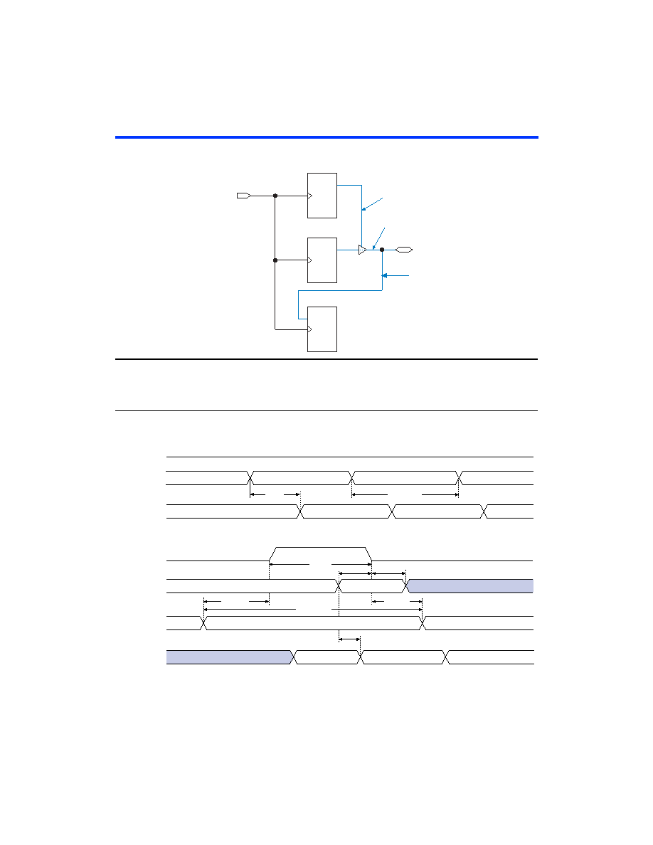
Figure 28. Synchronous Bidirectional Pin External Timing Model
waveforms, respectively, for the EAB macroparameters in Table 24.
Figure 29. EAB Asynchronous Timing Waveforms
PRN
CLRN
DQ
PRN
CLRN
DQ
PRN
CLRN
DQ
Dedicated
Clock
Bidirectional
Pin
Output Register
tINSUBIDIR
tOUTCOBIDIR
tXZBIDIR
tZXBIDIR
tINHBIDIR
OE Register
Input Register
EAB Asynchronous Write
EAB Asynchronous Read
WE
a0
d0
d3
tEABRCCOMB
a1
a2
a3
d2
tEABAA
d1
Address
Data-Out
WE
a0
din1
dout2
tEABDD
a1
a2
din1
din0
tEABWCCOMB
tEABWASU
tEABWAH
tEABWDH
tEABWDSU
tEABWP
din0
Data-In
Address
Data-Out
相關(guān)PDF資料 |
PDF描述 |
|---|---|
| EP1K50FI256-2 | IC ACEX 1K FPGA 50K 256-FBGA |
| EP1K50FC256-1N | IC ACEX 1K FPGA 50K 256-FBGA |
| A54SX32A-FFGG144 | IC FPGA SX 48K GATES 144-FBGA |
| A54SX32A-FFG144 | IC FPGA SX 48K GATES 144-FBGA |
| ABC50DREN-S13 | CONN EDGECARD 100PS .100 EYELET |
相關(guān)代理商/技術(shù)參數(shù) |
參數(shù)描述 |
|---|---|
| EP1K50FI256-2P | 制造商:未知廠家 制造商全稱(chēng):未知廠家 功能描述:Field Programmable Gate Array (FPGA) |
| EP1K50FI256-2X | 制造商:未知廠家 制造商全稱(chēng):未知廠家 功能描述:Field Programmable Gate Array (FPGA) |
| EP1K50FI256-3F | 制造商:未知廠家 制造商全稱(chēng):未知廠家 功能描述:Field Programmable Gate Array (FPGA) |
| EP1K50FI484-1DX | 制造商:未知廠家 制造商全稱(chēng):未知廠家 功能描述:Field Programmable Gate Array (FPGA) |
| EP1K50FI484-1F | 制造商:未知廠家 制造商全稱(chēng):未知廠家 功能描述:Field Programmable Gate Array (FPGA) |
發(fā)布緊急采購(gòu),3分鐘左右您將得到回復(fù)。