- 您現(xiàn)在的位置:買賣IC網(wǎng) > PDF目錄4482 > EP1K50FI256-2N (Altera)IC ACEX 1K FPGA 50K 256-FBGA PDF資料下載
參數(shù)資料
| 型號: | EP1K50FI256-2N |
| 廠商: | Altera |
| 文件頁數(shù): | 38/86頁 |
| 文件大小: | 0K |
| 描述: | IC ACEX 1K FPGA 50K 256-FBGA |
| 產(chǎn)品培訓(xùn)模塊: | Three Reasons to Use FPGA's in Industrial Designs |
| 標(biāo)準(zhǔn)包裝: | 90 |
| 系列: | ACEX-1K® |
| LAB/CLB數(shù): | 360 |
| 邏輯元件/單元數(shù): | 2880 |
| RAM 位總計: | 40960 |
| 輸入/輸出數(shù): | 186 |
| 門數(shù): | 199000 |
| 電源電壓: | 2.375 V ~ 2.625 V |
| 安裝類型: | 表面貼裝 |
| 工作溫度: | -40°C ~ 85°C |
| 封裝/外殼: | 256-BGA |
| 供應(yīng)商設(shè)備封裝: | 256-FBGA(17x17) |
第1頁第2頁第3頁第4頁第5頁第6頁第7頁第8頁第9頁第10頁第11頁第12頁第13頁第14頁第15頁第16頁第17頁第18頁第19頁第20頁第21頁第22頁第23頁第24頁第25頁第26頁第27頁第28頁第29頁第30頁第31頁第32頁第33頁第34頁第35頁第36頁第37頁當(dāng)前第38頁第39頁第40頁第41頁第42頁第43頁第44頁第45頁第46頁第47頁第48頁第49頁第50頁第51頁第52頁第53頁第54頁第55頁第56頁第57頁第58頁第59頁第60頁第61頁第62頁第63頁第64頁第65頁第66頁第67頁第68頁第69頁第70頁第71頁第72頁第73頁第74頁第75頁第76頁第77頁第78頁第79頁第80頁第81頁第82頁第83頁第84頁第85頁第86頁
Altera Corporation
43
ACEX 1K Programmable Logic Device Family Data Sheet
D
e
ve
lo
pm
e
n
t
13
To
o
ls
Notes to tables:
(1)
The most significant bit (MSB) is on the left.
(2)
The least significant bit (LSB) for all JTAG IDCODEs is 1.
ACEX 1K devices include weak pull-up resistors on the JTAG pins.
f For more information, see the following documents:
■
■
Jam Programming & Test Language Specification
Figure 20 shows the timing requirements for the JTAG signals.
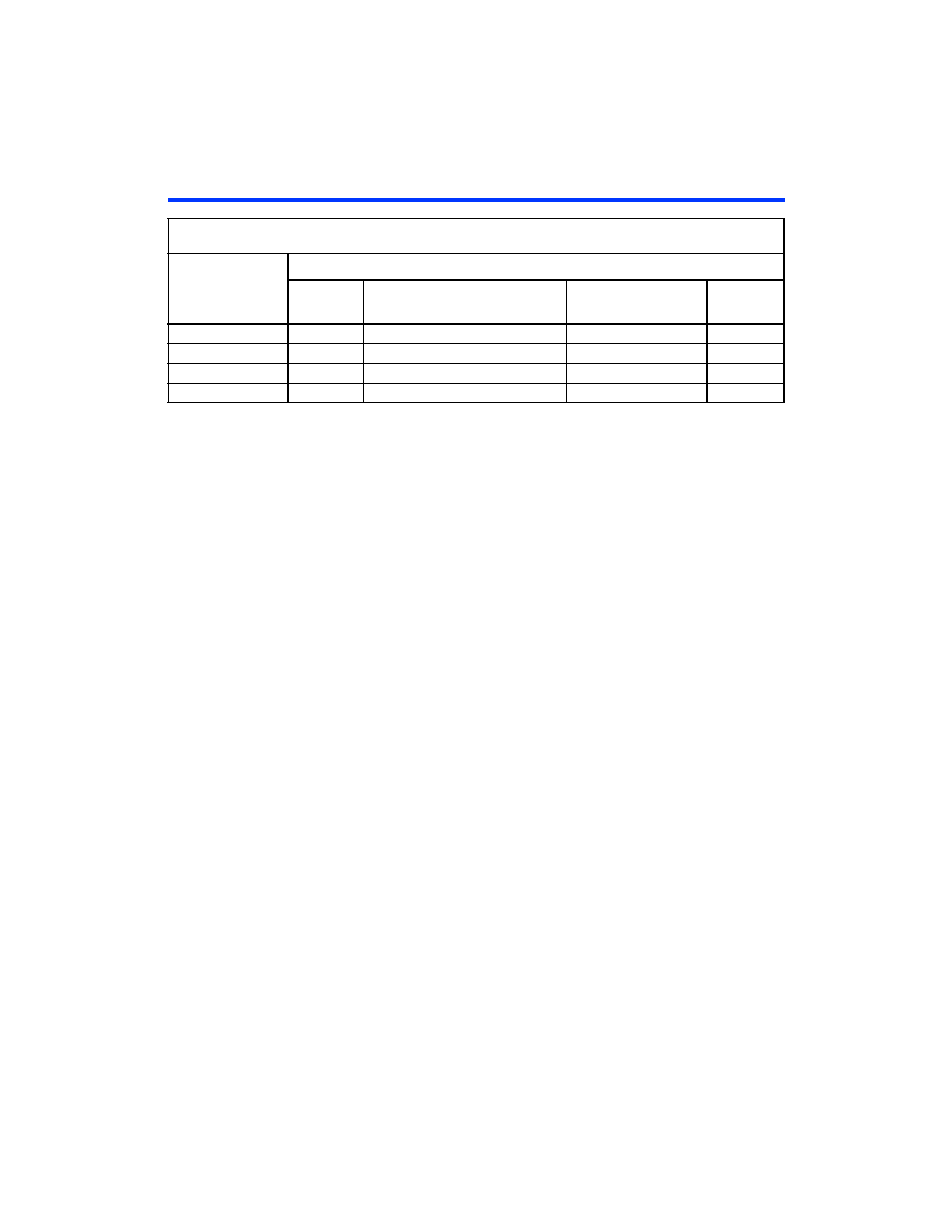
Table 16. 32-Bit IDCODE for ACEX 1K Devices
Device
IDCODE (32 Bits)
Version
(4 Bits)
Part Number (16 Bits)
Manufacturer’s
Identity (11 Bits)
1 (1 Bit) (2)
EP1K10
0001
0001 0000 0001 0000
00001101110
1
EP1K30
0001
0001 0000 0011 0000
00001101110
1
EP1K50
0001
0001 0000 0101 0000
00001101110
1
EP1K100
0010
0000 0001 0000 0000
00001101110
1
相關(guān)PDF資料 |
PDF描述 |
|---|---|
| EP1K50FI256-2 | IC ACEX 1K FPGA 50K 256-FBGA |
| EP1K50FC256-1N | IC ACEX 1K FPGA 50K 256-FBGA |
| A54SX32A-FFGG144 | IC FPGA SX 48K GATES 144-FBGA |
| A54SX32A-FFG144 | IC FPGA SX 48K GATES 144-FBGA |
| ABC50DREN-S13 | CONN EDGECARD 100PS .100 EYELET |
相關(guān)代理商/技術(shù)參數(shù) |
參數(shù)描述 |
|---|---|
| EP1K50FI256-2P | 制造商:未知廠家 制造商全稱:未知廠家 功能描述:Field Programmable Gate Array (FPGA) |
| EP1K50FI256-2X | 制造商:未知廠家 制造商全稱:未知廠家 功能描述:Field Programmable Gate Array (FPGA) |
| EP1K50FI256-3F | 制造商:未知廠家 制造商全稱:未知廠家 功能描述:Field Programmable Gate Array (FPGA) |
| EP1K50FI484-1DX | 制造商:未知廠家 制造商全稱:未知廠家 功能描述:Field Programmable Gate Array (FPGA) |
| EP1K50FI484-1F | 制造商:未知廠家 制造商全稱:未知廠家 功能描述:Field Programmable Gate Array (FPGA) |
發(fā)布緊急采購,3分鐘左右您將得到回復(fù)。