- 您現在的位置:買賣IC網 > PDF目錄375306 > AM49BDS640AHE9I (SPANSION LLC) Stacked Multichip Package (MCP), Flash Memory and pSRAM CMOS 1.8 Volt-only Simultaneous Read/Write PDF資料下載
參數資料
| 型號: | AM49BDS640AHE9I |
| 廠商: | SPANSION LLC |
| 元件分類: | 存儲器 |
| 英文描述: | Stacked Multichip Package (MCP), Flash Memory and pSRAM CMOS 1.8 Volt-only Simultaneous Read/Write |
| 中文描述: | SPECIALTY MEMORY CIRCUIT, PBGA89 |
| 封裝: | 10 X 8 MM, FBGA-89 |
| 文件頁數: | 41/84頁 |
| 文件大?。?/td> | 763K |
| 代理商: | AM49BDS640AHE9I |
第1頁第2頁第3頁第4頁第5頁第6頁第7頁第8頁第9頁第10頁第11頁第12頁第13頁第14頁第15頁第16頁第17頁第18頁第19頁第20頁第21頁第22頁第23頁第24頁第25頁第26頁第27頁第28頁第29頁第30頁第31頁第32頁第33頁第34頁第35頁第36頁第37頁第38頁第39頁第40頁當前第41頁第42頁第43頁第44頁第45頁第46頁第47頁第48頁第49頁第50頁第51頁第52頁第53頁第54頁第55頁第56頁第57頁第58頁第59頁第60頁第61頁第62頁第63頁第64頁第65頁第66頁第67頁第68頁第69頁第70頁第71頁第72頁第73頁第74頁第75頁第76頁第77頁第78頁第79頁第80頁第81頁第82頁第83頁第84頁
December 5, 2003
Am49BDS640AH
39
A D V A N C E I N F O R M A T I O N
WRITE OPERATION STATUS
The device provides several bits to determine the
status of a program or erase operation: DQ2, DQ3,
DQ5, DQ6, and DQ7.
Table 17, “Write Operation
Status,” on page 43
and the following subsections
describe the function of these bits. DQ7 and DQ6 each
offers a method for determining whether a program or
erase operation is complete or in progress.
DQ7: Data# Polling
The Data# Polling bit, DQ7, indicates to the host
system whether an Embedded Program or Erase algo-
rithm is in progress or completed, or whether a bank is
in Erase Suspend. Data# Polling is valid after the rising
edge of the final WE# pulse in the command sequence.
During the Embedded Program algorithm, the device
outputs on DQ7 the complement of the datum pro-
grammed to DQ7. This DQ7 status also applies to pro-
gramming during Erase Suspend. When the
Embedded Program algorithm is complete, the device
outputs the datum programmed to DQ7. The system
must provide the program address to read valid status
information on DQ7. If a program address falls within a
protected sector, Data# Polling on DQ7 is active for
approximately 1 μs, then that bank returns to the read
mode.
During the Embedded Erase algorithm, Data# Polling
produces a “0” on DQ7. When the Embedded Erase
algorithm is complete, or if the bank enters the Erase
Suspend mode, Data# Polling produces a “1” on DQ7.
The system must provide an address within any of the
sectors selected for erasure to read valid status infor-
mation on DQ7.
After an erase command sequence is written, if all
sectors selected for erasing are protected, Data#
Polling on DQ7 is active for approximately 100 μs, then
the bank returns to the read mode. If not all selected
sectors are protected, the Embedded Erase algorithm
erases the unprotected sectors, and ignores the
selected sectors that are protected. However, if the
system reads DQ7 at an address within a protected
sector, the status may not be valid.
Just prior to the completion of an Embedded Program
or Erase operation, DQ7 may change asynchronously
with DQ6–DQ0 while Output Enable (OE#) is asserted
low. That is, the device may change from providing
status information to valid data on DQ7. Depending on
when the system samples the DQ7 output, it may read
the status or valid data. Even if the device has com-
pleted the program or erase operation and DQ7 has
valid data, the data outputs on DQ6-DQ0 may be still
invalid. Valid data on DQ7-DQ0 will appear on succes-
sive read cycles.
Table 17, “Write Operation Status,” on page 43
shows
the outputs for Data# Polling on DQ7.
Figure 6, “Data#
Polling Algorithm,” on page 39
shows the Data# Polling
algorithm.
Figure 37, “Data# Polling Timings
(During Embedded Algorithm),” on page 67
in the AC
Characteristics section shows the Data# Polling timing
diagram.
Notes:
1. VA = Valid address for programming. During a sector
erase operation, a valid address is any sector address
within the sector being erased. During chip erase, a valid
address is any non-protected sector address.
2. DQ7 should be rechecked even if DQ5 = “1” because
DQ7 may change simultaneously with DQ5.
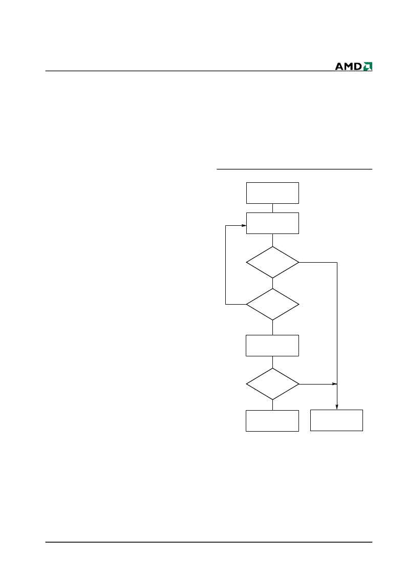
Figure 6.
Data# Polling Algorithm
DQ7 = Data
Yes
No
No
DQ5 = 1
No
Yes
Yes
FAIL
PASS
Read DQ7–DQ0
Addr = VA
Read DQ7–DQ0
Addr = VA
DQ7 = Data
START
相關PDF資料 |
PDF描述 |
|---|---|
| AM49DL320BGT701 | Stacked Multi-Chip Package (MCP) Flash Memory and SRAM 32 Megabit (4 M x 8-Bit/2 M x 16-Bit) CMOS 3.0 Volt-only, Simultaneous |
| AM49DL320BGB701 | Stacked Multi-Chip Package (MCP) Flash Memory and SRAM 32 Megabit (4 M x 8-Bit/2 M x 16-Bit) CMOS 3.0 Volt-only, Simultaneous |
| AM49DL320BGB70IS | Stacked Multi-Chip Package (MCP) Flash Memory and SRAM 32 Megabit (4 M x 8-Bit/2 M x 16-Bit) CMOS 3.0 Volt-only, Simultaneous |
| AM49DL320BGB70IT | Stacked Multi-Chip Package (MCP) Flash Memory and SRAM 32 Megabit (4 M x 8-Bit/2 M x 16-Bit) CMOS 3.0 Volt-only, Simultaneous |
| AM49DL320BGB851 | Stacked Multi-Chip Package (MCP) Flash Memory and SRAM 32 Megabit (4 M x 8-Bit/2 M x 16-Bit) CMOS 3.0 Volt-only, Simultaneous |
相關代理商/技術參數 |
參數描述 |
|---|---|
| AM49DL3208G | 制造商:未知廠家 制造商全稱:未知廠家 功能描述:Am49DL3208G - Stacked Multi-Chip Package (MCP) Flash Memory and pSRAM |
| AM49DL320BG | 制造商:未知廠家 制造商全稱:未知廠家 功能描述:Am49DL320BG - Stacked Multi-Chip Package (MCP) Flash Memory and SRAM |
| AM49DL320BGB701 | 制造商:SPANSION 制造商全稱:SPANSION 功能描述:Stacked Multi-Chip Package (MCP) Flash Memory and SRAM 32 Megabit (4 M x 8-Bit/2 M x 16-Bit) CMOS 3.0 Volt-only, Simultaneous |
| AM49DL320BGB701S | 制造商:AMD 制造商全稱:Advanced Micro Devices 功能描述:32 Megabit (4 M x 8-Bit/2 M x 16-Bit) CMOS 3.0 Volt-only, Simultaneous Operation Flash Memory and 32 Mbit (2M x 16-Bit) Pseudo Static RAM |
| AM49DL320BGB701T | 制造商:AMD 制造商全稱:Advanced Micro Devices 功能描述:32 Megabit (4 M x 8-Bit/2 M x 16-Bit) CMOS 3.0 Volt-only, Simultaneous Operation Flash Memory and 32 Mbit (2M x 16-Bit) Pseudo Static RAM |
發(fā)布緊急采購,3分鐘左右您將得到回復。