- 您現(xiàn)在的位置:買(mǎi)賣(mài)IC網(wǎng) > PDF目錄373980 > ADE7758ARWZRL (ANALOG DEVICES INC) Poly Phase Multifunction Energy Metering IC with Per Phase Information PDF資料下載
參數(shù)資料
| 型號(hào): | ADE7758ARWZRL |
| 廠商: | ANALOG DEVICES INC |
| 元件分類(lèi): | 模擬信號(hào)調(diào)理 |
| 英文描述: | Poly Phase Multifunction Energy Metering IC with Per Phase Information |
| 中文描述: | SPECIALTY ANALOG CIRCUIT, PDSO24 |
| 封裝: | LEAD FREE, MS-013-AD, SOIC-24 |
| 文件頁(yè)數(shù): | 54/68頁(yè) |
| 文件大小: | 1584K |
| 代理商: | ADE7758ARWZRL |
第1頁(yè)第2頁(yè)第3頁(yè)第4頁(yè)第5頁(yè)第6頁(yè)第7頁(yè)第8頁(yè)第9頁(yè)第10頁(yè)第11頁(yè)第12頁(yè)第13頁(yè)第14頁(yè)第15頁(yè)第16頁(yè)第17頁(yè)第18頁(yè)第19頁(yè)第20頁(yè)第21頁(yè)第22頁(yè)第23頁(yè)第24頁(yè)第25頁(yè)第26頁(yè)第27頁(yè)第28頁(yè)第29頁(yè)第30頁(yè)第31頁(yè)第32頁(yè)第33頁(yè)第34頁(yè)第35頁(yè)第36頁(yè)第37頁(yè)第38頁(yè)第39頁(yè)第40頁(yè)第41頁(yè)第42頁(yè)第43頁(yè)第44頁(yè)第45頁(yè)第46頁(yè)第47頁(yè)第48頁(yè)第49頁(yè)第50頁(yè)第51頁(yè)第52頁(yè)第53頁(yè)當(dāng)前第54頁(yè)第55頁(yè)第56頁(yè)第57頁(yè)第58頁(yè)第59頁(yè)第60頁(yè)第61頁(yè)第62頁(yè)第63頁(yè)第64頁(yè)第65頁(yè)第66頁(yè)第67頁(yè)第68頁(yè)
ADE7758
Example—Calibration of RMS Offsets
For this example,
I
TEST
= 10 A,
I
MAX
= 100 A,
V
NOM
= 220 V,
V
FULLSCALE
= 500 V,
Power Factor
= 1, and
Frequency
= 50 Hz.
Rev. A | Page 54 of 68
With
I
TEST
and
V
NOM
, the example ADE7758 meter shows
0x34266 in the AIRMS (0x0A) register and 0x10B0A3 in the
AVRMS (0x0D) register. At I
MAX/500
, the example meter shows
0x19F in AIRMS. At V
NOM/20
,
the example meter shows 0xD65B
in the AVRMS register. These are the average value of 20
samples synchronous to the zero crossings of all three phases.
Using this data, 3d is written to AVRMSOS (0x33) and 1004d
is written to AIRMSOS (0x36) registers according to the
Equation 56 and Equation 57.
×
,
2
=
384
16
) (
2
1
xIRMSOS
(
10
×
)
(
)
1104
88
.
1103
10
–
606
,
213
–
415
2
2
2
2
2
=
=
×
(
) (
–
11
)
(
)
3
047
.
220
795
,
093
,
11
–
54875
220
64
1
=
=
×
×
×
=
xVRMSOS
This example shows the calculations and measurements for
Phase A only. However, all three xIRMS and xVRMS registers
can be read simultaneously to compute the values for each
xIRMSOS and xVRMSOS register.
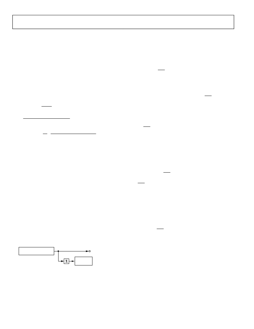
CHECKSUM REGISTER
The ADE7758 has a checksum register CHECKSUM[7:0]
(0x7E) to ensure the data bits received in the last serial read
operation are not corrupted. The 8-bit checksum register is
reset before the first bit (MSB of the register to be read) is put
on the DOUT pin. During a serial read operation, when each
data bit becomes available on the rising edge of SCLK, the bit is
added to the checksum register. In the end of the serial read
operation, the content of the checksum register is equal to the
sum of all the ones in the register previously read. Using the
checksum register, the user can determine if an error has
occurred during the last read operation. Note that a read to the
checksum register also generates a checksum of the checksum
register itself.
0
DOUT
ADDR: 0x7E
CHECKSUM
REGISTER
CONTENT OF REGISTERS
(N-BYTES)
Figure 85. Checksum Register for Serial Interface Read
ADE7758 INTERRUPTS
The ADE7758 interrupts are managed through the interrupt
status register (STATUS[23:0], Address 0x19) and the interrupt
mask register (MASK[23:0], Address 0x18). When an interrupt
event occurs in the ADE7758, the corresponding flag in the
interrupt status register is set to a Logic 1 (see Table 20). If the
mask bit for this interrupt in the interrupt mask register is
Logic 1, then the IRQ logic output goes active low. The flag bits
in the interrupt status register are set irrespective of the state of
the mask bits. To determine the source of the interrupt, the
system master (MCU) should perform a read from the reset
interrupt status register with reset. This is achieved by carrying
out a read from RSTATUS, Address 0x1A. The IRQ output goes
logic high on completion of the interrupt status register read
command (see the Interrupt Timing section). When carrying
out a read with reset, the ADE7758 is designed to ensure that no
interrupt events are missed. If an interrupt event occurs just as
the interrupt status register is being read, the event is not lost
and the IRQ logic output is guaranteed to go logic high for the
duration of the interrupt status register data transfer before
going logic low again to indicate the pending interrupt. Note
that the reset interrupt bit in the status register is high for only
one clock cycle; then it goes back to 0.
USING THE ADE7758 INTERRUPTS WITH AN MCU
Figure 87 shows a timing diagram that illustrates a suggested
implementation of ADE7758 interrupt management using an
MCU. At time
t
1
,
the IRQ line goes active low indicating that
one or more interrupt events have occurred in the ADE7758.
The IRQ logic output should be tied to a negative edge triggered
external interrupt on the MCU. On detection of the negative
edge, the MCU should be configured to start executing its
interrupt service routine (ISR). On entering the ISR, all
interrupts should be disabled using the global interrupt mask
bit. At this point, the MCU external interrupt flag can be
cleared in order to capture interrupt events that occur during
the current ISR. When the MCU interrupt flag is cleared, a read
from the reset interrupt status register with reset is carried out.
(This causes the IRQ line to be reset logic high (
t
2
)—see the
Interrupt Timing section.) The reset interrupt status register
contents are used to determine the source of the interrupt(s) and
hence the appropriate action to be taken. If a subsequent
interrupt event occurs during the ISR (
t
3
) that event is recorded
by the MCU external interrupt flag being set again. On
returning from the ISR, the global interrupt mask bit is cleared
(same instruction cycle) and the external interrupt flag uses the
MCU to jump to its ISR once again. This ensures that the MCU
does not miss any external interrupts. The reset bit in the status
register is an exception to this, and is only high for one clock
cycle after a reset event.
相關(guān)PDF資料 |
PDF描述 |
|---|---|
| ADE7759ARSRL | Active Energy Metering IC with di/dt Sensor Interface |
| ADE7759ARS | 8-Channel 14-Bit Single-Supply Voltage-Output DAC; Package: LQFP (10x10mm); No of Pins: 52; Temperature Range: Industrial |
| ADE7759 | Active Energy Metering IC with di/dt Sensor Interface |
| ADE7760ARSRL | Energy Metering IC with On-Chip Fault Detection |
| ADE7760 | 8-Channel 14-Bit Single-Supply Voltage-Output DAC; Package: LQFP (10x10mm); No of Pins: 52; Temperature Range: Industrial |
相關(guān)代理商/技術(shù)參數(shù) |
參數(shù)描述 |
|---|---|
| ADE7759 | 制造商:AD 制造商全稱(chēng):Analog Devices 功能描述:Active Energy Metering IC with di/dt Sensor Interface |
| ADE7759ARS | 功能描述:IC ENERGY METERING 1PHASE 20SSOP RoHS:否 類(lèi)別:集成電路 (IC) >> PMIC - 能量測(cè)量 系列:- 產(chǎn)品培訓(xùn)模塊:Lead (SnPb) Finish for COTS Obsolescence Mitigation Program 標(biāo)準(zhǔn)包裝:2,500 系列:* |
| ADE7759ARSRL | 功能描述:IC ENERGY METERING 1PHASE 20SSOP RoHS:否 類(lèi)別:集成電路 (IC) >> PMIC - 能量測(cè)量 系列:- 產(chǎn)品培訓(xùn)模塊:Lead (SnPb) Finish for COTS Obsolescence Mitigation Program 標(biāo)準(zhǔn)包裝:2,500 系列:* |
| ADE7759ARSZ | 功能描述:IC ENERGY METERING 1PHASE 20SSOP RoHS:是 類(lèi)別:集成電路 (IC) >> PMIC - 能量測(cè)量 系列:- 產(chǎn)品培訓(xùn)模塊:Lead (SnPb) Finish for COTS Obsolescence Mitigation Program 標(biāo)準(zhǔn)包裝:2,500 系列:* |
| ADE7759ARSZRL | 功能描述:IC ENERGY METERING 1PHASE 20SSOP RoHS:是 類(lèi)別:集成電路 (IC) >> PMIC - 能量測(cè)量 系列:- 產(chǎn)品培訓(xùn)模塊:Lead (SnPb) Finish for COTS Obsolescence Mitigation Program 標(biāo)準(zhǔn)包裝:2,500 系列:* |
發(fā)布緊急采購(gòu),3分鐘左右您將得到回復(fù)。