- 您現(xiàn)在的位置:買賣IC網(wǎng) > PDF目錄373980 > ADE7753 (Analog Devices, Inc.) Active and Apparent Energy Metering IC with di/dt sensor interface PDF資料下載
參數(shù)資料
| 型號: | ADE7753 |
| 廠商: | Analog Devices, Inc. |
| 英文描述: | Active and Apparent Energy Metering IC with di/dt sensor interface |
| 中文描述: | 主動與迪視電能計量IC / dt的傳感器接口 |
| 文件頁數(shù): | 21/38頁 |
| 文件大小: | 449K |
| 代理商: | ADE7753 |
第1頁第2頁第3頁第4頁第5頁第6頁第7頁第8頁第9頁第10頁第11頁第12頁第13頁第14頁第15頁第16頁第17頁第18頁第19頁第20頁當前第21頁第22頁第23頁第24頁第25頁第26頁第27頁第28頁第29頁第30頁第31頁第32頁第33頁第34頁第35頁第36頁第37頁第38頁
ADE7753
–21–
REV. PrF 10/02
PRELIMINARY TECHNICAL DATA
POWE R OFFSE T CALIBRAT ION
T he ADE7753 also incorporates an Active Power Offset
register (APOS[15:0]). T his is a signed 2’s complement 16-
bit register which can be used to remove offsets in the active
power calculation—
see Figure 33
. An offset may exist in the
power calculation due to cross talk between channels on the
PCB or in the IC itself. T he offset calibration will allow the
contents of the Active Power register to be maintained at zero
when no power is being consumed.
T wo hundred fifty six LSBs (APOS=0100h) written to the
Active Power Offset register are equivalent to 1 LSB in the
Waveform Sample register. Assuming the average value
outputs from LPF2 is CCCCDh (838,861 in Decimal) when
inputs on Channels 1 and 2 are both at full-scale. At -60dB
down on C hannel 1 (1/1000 of the C hannel 1 full-scale
input), the average word value outputs from LPF2 is 838.861
(838,861/1,000). 1 LSB in the LPF2 output has a measure-
ment error of 1/838.861
×
100% = 0.119% of the average
value. T he Active Power Offset register has a resolution
equal to 1/256 L SB of the Waveform register, hence the
power offset correction resolution is 0.00047%/LSB (0.119%/
256) at -60dB.
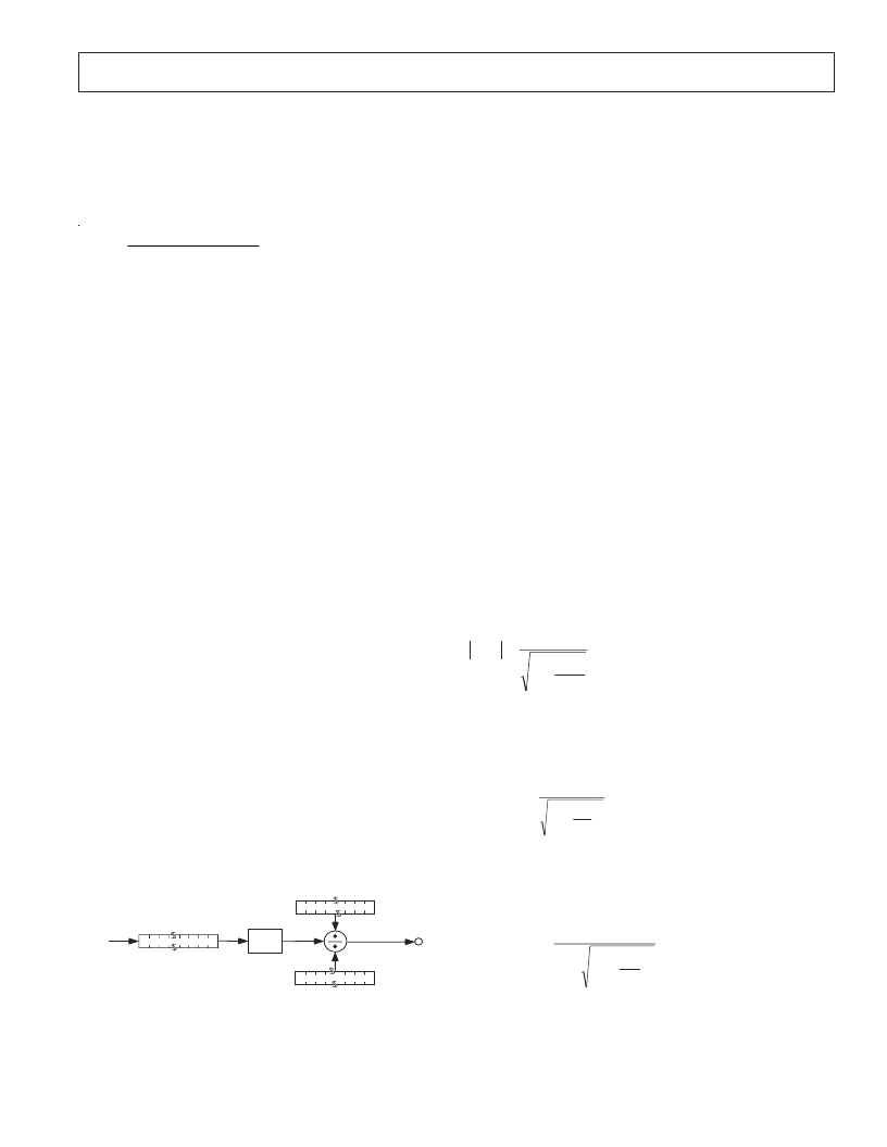
E NE RGY T O FRE QUE NCY CONVE RSION
ADE7753 also provides energy to frequency conversion for
calibration purposes. After initial calibration at manufactur-
ing, the manufacturer or end customer will often verify the
energy meter calibration. One convenient way to verify the
meter calibration is for the manufacturer to provide an output
frequency which is proportional to the energy or active power
under steady load conditions. T his output frequency can
provide a simple, single wire, optically isolated interface to
external calibration equipment. F igure 37 illustrates the
Energy-to-Frequency conversion in the ADE7753.
CF
0
11
CFNUM[11:0]
Energy
0
11
CFDEN[11:0]
DFC
0
23
AENERGY[23:0]
Figure 37– ADE7753 Energy to Frequency Conversion
A Digital to Frequency Converter (DFC) is used to generate
the CF pulsed output. T he DFC generates a pulse each time
one LSB in the Active Energy register is accumulated. An
output pulse is generated when (CFDEN+1)/(CFNUM+1)
number of pulses are generated at the DFC output. Under
steady load conditions the output frequency is proportional to
the Active Power.
T he maximum output frequency, with AC input signals at
full-scale and C FNUM=00h & C FDEN=00h, is approxi-
mately 23 kHz.
T he ADE7753 incorporates two registers, C FNUM[11:0]
and C F DEN[11:0], to set the C F frequency. T hese are
unsigned 12-bit registers which can be used to adjust the CF
frequency to a wide range of values. T hese frequency scaling
registers are 12-bit registers which can scale the output
frequency by 1/2
12
to 1 with a step of 1/2
12
.
If the value zero is written to any of these registers, the value
one would be applied to the register. T he ratio (CFNUM+1)/
(CFDEN+1) should be smaller than one to assure proper
operation. If the ratio of the registers (C F NU M +1)/
(CFDEN+1) is greater than one, the register values would
be adjust to a ratio (CFNUM+1)/(CFDEN+1) of one.
For example if the output frequency is 1.562kHz while the
contents of CFDENare zero (000h), then the output frequency
can be set to 6.1Hz by writing FFh to the CFDEN register.
Note that for values where C F D E N>C F NU M , the
performance of the CF frequency is not guaranteed. CFNUM
should always be set to a value less than CFDEN.
T he output frequency will have a slight ripple at a frequency
equal to twice the line frequency. T his is due to imperfect
filtering of the instantaneous power signal to generate the
Active Power signal – see
Active Power Calculation
. Equation 3
gives an expression for the instantaneous power signal. T his
is filtered by LPF2 which has a magnitude response given by
Equation 9.
1
)
(
f
+
2
2
9
1
f
H
=
(9)
T he Active Power signal (output of LPF2) can be rewritten
as.
(
)
t
f
f
VI
VI
t
p
l
l
π
4
cos
9
2
1
)
(
2
+
=
(10)
where
f
l
is the line frequency (e.g., 60Hz)
From Equation 6
(
)
t
f
f
f
VI
VIt
t
E
l
l
l
π
π
4
sin
9
2
1
4
)
(
2
+
=
(11)
From Equation 11 it can be seen that there is a small ripple
in the energy calculation due to a sin(2
ω
t) component. T his
is shown graphically in F igure 38. T he Active E nergy
calculation is shown by the dashed straight line and is equal
With full-scale sinusoidal signals on the analog inputs and the
WGAIN register set to 000h, the average word value from
each L PF2 is C C C C Dh - see Figure 31. T he maximum
positive value which can be stored in the internal 47-bit
register is 2
46
- 1 or 7FFF,FFFF,FFFFh before it overflows,
the integration time under these conditions with WDIV=0 is
calculated as follows:
s
s
s
μ
CCCCDh
FFFFh
FFFF
FFF
3
Time
min
12
.
=
5
187
=
12
.
×
,
,
=
When WDIV is set to a value different from 0, the integration
time varies as shown on Equation 8.
T ime = T ime
WDIV=0
x WDIV
(8)
相關PDF資料 |
PDF描述 |
|---|---|
| ADE7753ARS | Active and Apparent Energy Metering IC with di/dt sensor interface |
| ADE7753ARSRL | Active and Apparent Energy Metering IC with di/dt sensor interface |
| ADE7754 | ADE7754 |
| ADE7754AR | ADE7754 |
| ADE7754ARRL | ADE7754 |
相關代理商/技術參數(shù) |
參數(shù)描述 |
|---|---|
| ADE7753_10 | 制造商:AD 制造商全稱:Analog Devices 功能描述:Single-Phase Multifunction Metering IC with di/dt Sensor Interface |
| ADE7753ARS | 制造商:Analog Devices 功能描述:Single Phase Multifunction Metering IC 20-Pin SSOP 制造商:Rochester Electronics LLC 功能描述:- Bulk 制造商:Analog Devices 功能描述:IC SEMICONDUTOR ((NS)) |
| ADE7753ARSRL | 制造商:Analog Devices 功能描述:Single Phase Multifunction Metering IC 20-Pin SSOP T/R 制造商:Rochester Electronics LLC 功能描述:- Bulk |
| ADE7753ARSZ | 功能描述:IC ENERGY METERING 1PHASE 20SSOP RoHS:是 類別:集成電路 (IC) >> PMIC - 能量測量 系列:- 產(chǎn)品培訓模塊:Lead (SnPb) Finish for COTS Obsolescence Mitigation Program 標準包裝:2,500 系列:* |
| ADE7753ARSZ | 制造商:Analog Devices 功能描述:ENERGY METERING IC |
發(fā)布緊急采購,3分鐘左右您將得到回復。