- 您現(xiàn)在的位置:買賣IC網 > PDF目錄373980 > ADE7753 (Analog Devices, Inc.) Active and Apparent Energy Metering IC with di/dt sensor interface PDF資料下載
參數(shù)資料
| 型號: | ADE7753 |
| 廠商: | Analog Devices, Inc. |
| 英文描述: | Active and Apparent Energy Metering IC with di/dt sensor interface |
| 中文描述: | 主動與迪視電能計量IC / dt的傳感器接口 |
| 文件頁數(shù): | 17/38頁 |
| 文件大小: | 449K |
| 代理商: | ADE7753 |
第1頁第2頁第3頁第4頁第5頁第6頁第7頁第8頁第9頁第10頁第11頁第12頁第13頁第14頁第15頁第16頁當前第17頁第18頁第19頁第20頁第21頁第22頁第23頁第24頁第25頁第26頁第27頁第28頁第29頁第30頁第31頁第32頁第33頁第34頁第35頁第36頁第37頁第38頁
ADE7753
–17–
REV. PrF 10/02
PRELIMINARY TECHNICAL DATA
directly to the multiplier and is not filtered. A HPF is not
required to remove any DC offset since it is only required to
remove the offset from one channel to eliminate errors due to
offsets in the power calculation. When in waveform sample
mode, one of four output sample rates can be chosen by using
bits 11 and 12 of the Mode register. T he available output
sample rates are 27.9kSPS, 14kSPS, 7kSPS or 3.5kSPS—
see
Mode Register
. T he interrupt request output
IRQ
signals a
sample availability by going active low. T he timing is the
same as that for Channel 1 and is shown in Figure 22.
Channel 2 RMS calculation
Figure 26 shows the details of the signal processing chain for
the RMS calculation on Channel 2. T he channel 2 RMS
value is processed from the samples used in the channel 2
waveform sampling mode. T he RMS value will be slightly
attenuated because of LPF1. Channel 2 RMS value is stored
in the unsigned 24-bit VRMS register. T he update rate of the
channel 2 RMS measurement is CLK IN/4.
With the specified full scale AC analog input signal of 0.5V,
the outputs from the L PF 1 swings between 2518h and
DAE8h at 60 Hz- see
Channel 2 ADC
. T he equivalent RMS
value of this full-scale AC signal is approximately 1,561,400
(17D338h) in the VRMS register.
LPF3
Voltage Signal - V(t)
2518h
0h
DAE8h
VRMS[23:0]
17D338h
00h
Channel 2
LPF1
S
SGN2928
222120
VRMSOS[11:0]
Figure 26 - Channel 2 RMS signal processing
Channel 2 RMS offset compensation
T he ADE7753 incorporates a channel 2 RMS offset compen-
sation register (VRMSOS). T his is a 12-bit signed registers
which can be used to remove offset in the channel 2 RMS
calculation. An offset may exist in the RMS calculation due
to input noises and dc offset in the input samples. T he offset
calibration allows the contents of the VRMS register to be
maintained at zero when no voltage is applied.
1 LSB of the channel 2 RMS offset are equivalent to 1 LSB
of the RMS register. Assuming that the maximum value from
the channel 2 RMS calculation is 1,561,400d with full scale
AC inputs, then 1 LSB of the channel 2 RMS offset represents
0.064% of measurement error at -60dB down of full scale.
VRMSOS
V
V
rmso
rms
+
=
where V
rmso
is the RMS measurement without offset correc-
tion.
PHASE COMPE NSAT ION
When the HPF is disabled, the phase error between Channel
1 and Channel 2 is zero from DC to 3.5kHz. When HPF is
enabled, C hannel 1 has a phase response illustrated in
Figures 28 & 29. Also shown in Figure 30 is the magnitude
response of the filter. As can be seen from the plots, the phase
response is almost zero from 45Hz to 1kHz, T his is all that
is required in typical energy measurement applications.
C HANNE L 2 AD C
Channel 2 Sampling
In Channel 2 waveform sampling mode (MODE[14:13] =
1,1 and WSMP = 1) the ADC output code scaling for
Channel 2 is not the same as Channel 1. Channel 2 waveform
sample is a 16-bit word and sign extended to 24 bits. For
normal operation, the differential voltage signal between
V2P and V2N should not exceed 0.5V. With maximum
voltage input (±0.5V at PGA gain of 1), the outputs from the
ADC swings between 2852h and D7AEh (±10,322 Deci-
mal). However, before being passed to the Waveform register,
the ADC output is passed through a single pole, low pass
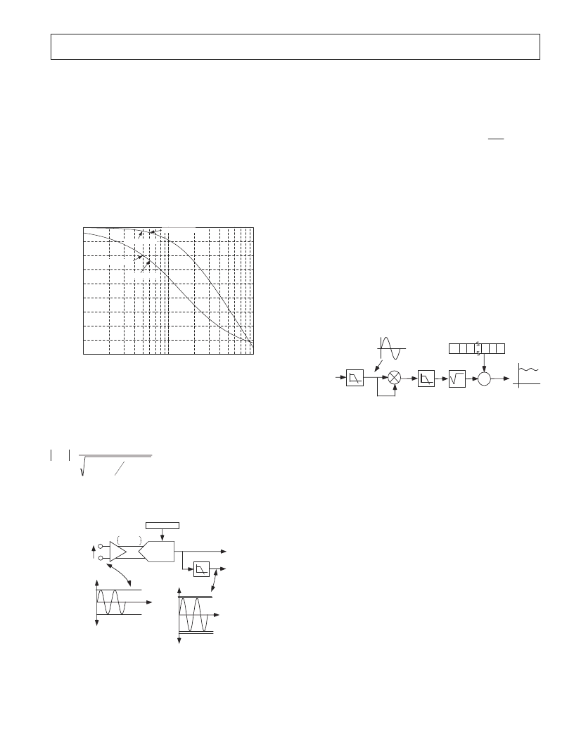
filter with a cutoff frequency of 140Hz. T he plots in Figure
24 shows the magnitude and phase response of this filter.
10
1
10
2
10
3
-90
-80
-70
-60
-50
-40
-30
-20
-10
0
-18
-16
-14
-12
-10
-8
-6
-4
-2
0
G
P
Frequency (Hz)
60 Hz, -0.73dB
50 Hz, -0.52dB
60 Hz, -23.2°
50 Hz, -19.7°
Figure 24 – Magnitude & Phase response of LPF1
T he L PF 1 has the effect of attenuating the signal. F or
example if the line frequency is 60Hz, then the signal at the
output of LPF1 will be attenuated by about 8%.
(
)
0.73dB
0.919
140Hz
60Hz
1
1
H(f)
2
=
=
+
=
Note LPF1 does not affect the power calculation. T he signal
processing chain in Channel 2 is illustrated in Figure 25.
V2P
V2N
ADC 2
PGA2
x1, x2, x4,
x8, x16
GAIN[7:5]
REFERENCE
V2
V1
0V
Analog
Input Range
0.5V, 0.25V, 0.125V,
62.5mV, 31.25mV
ACTIVE AND REACTIVE
ENERGY CALCULATION
LPF1
0000h
2852h
D7AEh
LPF Output
word Range
VRMS CALCULATION
AND WAVEFORM
SAMPLING
(PEAK/SAG/ZX)
DAE8h
2.42V
Figure 25 – ADC and Signal Processing in Channel 2
Unlike Channel 1, Channel 2 has only one analog input range
(1V differential). However like Channel 1, Channel 2 does
have a PGA with gain selections of 1, 2, 4, 8 and 16. For
energy measurement, the output of the AD C is passed
相關PDF資料 |
PDF描述 |
|---|---|
| ADE7753ARS | Active and Apparent Energy Metering IC with di/dt sensor interface |
| ADE7753ARSRL | Active and Apparent Energy Metering IC with di/dt sensor interface |
| ADE7754 | ADE7754 |
| ADE7754AR | ADE7754 |
| ADE7754ARRL | ADE7754 |
相關代理商/技術參數(shù) |
參數(shù)描述 |
|---|---|
| ADE7753_10 | 制造商:AD 制造商全稱:Analog Devices 功能描述:Single-Phase Multifunction Metering IC with di/dt Sensor Interface |
| ADE7753ARS | 制造商:Analog Devices 功能描述:Single Phase Multifunction Metering IC 20-Pin SSOP 制造商:Rochester Electronics LLC 功能描述:- Bulk 制造商:Analog Devices 功能描述:IC SEMICONDUTOR ((NS)) |
| ADE7753ARSRL | 制造商:Analog Devices 功能描述:Single Phase Multifunction Metering IC 20-Pin SSOP T/R 制造商:Rochester Electronics LLC 功能描述:- Bulk |
| ADE7753ARSZ | 功能描述:IC ENERGY METERING 1PHASE 20SSOP RoHS:是 類別:集成電路 (IC) >> PMIC - 能量測量 系列:- 產品培訓模塊:Lead (SnPb) Finish for COTS Obsolescence Mitigation Program 標準包裝:2,500 系列:* |
| ADE7753ARSZ | 制造商:Analog Devices 功能描述:ENERGY METERING IC |
發(fā)布緊急采購,3分鐘左右您將得到回復。