- 您現(xiàn)在的位置:買賣IC網(wǎng) > PDF目錄373972 > AD9957BSVZ (ANALOG DEVICES INC) 1 GSPS Quadrature Digital Upconverter with 18-Bit IQ Data Path and 14-Bit DAC PDF資料下載
參數(shù)資料
| 型號(hào): | AD9957BSVZ |
| 廠商: | ANALOG DEVICES INC |
| 元件分類: | 通信及網(wǎng)絡(luò) |
| 英文描述: | 1 GSPS Quadrature Digital Upconverter with 18-Bit IQ Data Path and 14-Bit DAC |
| 中文描述: | SPECIALTY TELECOM CIRCUIT, PQFP100 |
| 封裝: | ROHS COMPLIANT, MS-026AED-HD, TQFP-100 |
| 文件頁數(shù): | 34/60頁 |
| 文件大小: | 840K |
| 代理商: | AD9957BSVZ |
第1頁第2頁第3頁第4頁第5頁第6頁第7頁第8頁第9頁第10頁第11頁第12頁第13頁第14頁第15頁第16頁第17頁第18頁第19頁第20頁第21頁第22頁第23頁第24頁第25頁第26頁第27頁第28頁第29頁第30頁第31頁第32頁第33頁當(dāng)前第34頁第35頁第36頁第37頁第38頁第39頁第40頁第41頁第42頁第43頁第44頁第45頁第46頁第47頁第48頁第49頁第50頁第51頁第52頁第53頁第54頁第55頁第56頁第57頁第58頁第59頁第60頁
AD9957
Rev. 0 | Page 34 of 60
0
TERMINATION
REF_CLK
DIFFERENTIAL SOURCE,
DIFFERENTIAL INPUT.
SINGLE-ENDED SOURCE,
DIFFERENTIAL INPUT.
SINGLE-ENDED SOURCE,
SINGLE-ENDED INPUT.
90
91
0.1μF
0.1μF
PECL,
LVPECL,
OR
LVDS
DRIVER
REF_CLK
90
91
50
0.1μF
0.1μF
BALUN
(1:1)
REF_CLK
REF_CLK
REF_CLK
REF_CLK
90
91
0.1μF
0.1μF
50
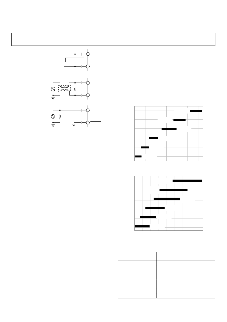
Figure 49. Direct Connection Diagram
PHASE-LOCKED LOOP (PLL) MULTIPLIER
An internal phase-locked loop (PLL) provides users of the
AD9957 the option to use a reference clock frequency that is
significantly lower than the system clock frequency. The PLL
supports a wide range of programmable frequency multiplica-
tion factors (12× to 127×) as well as a programmable charge
pump current and external loop filter components (connected
via the PLL_LOOP_FILTER pin). These features add an extra
layer of flexibility to the PLL, allowing optimization of phase
noise performance and flexibility in frequency plan develop-
ment. The PLL is also equipped with a PLL_LOCK pin.
The PLL output frequency range (f
SYSCLK
) is constrained to the
range of 420 MHz ≤ f
SYSCLK
≤ 1 GHz by the internal VCO. In
addition, the user must program the VCO to one of six operating
ranges such that f
SYSCLK
falls within the specified range. Figure 50
and Figure 51 summarize these VCO ranges.
Figure 50 shows the boundaries of the VCO frequency ranges
over the full range of temperature and supply voltage variation
for all devices from the available population. The implication is
that multiple devices chosen at random from the population and
operated under widely varying conditions may require different
values to be programmed into CFR3<26:24> to operate at the
same frequency. For example, Part A chosen randomly from the
population, operating in an ambient temperature of 10°C with
a system clock frequency of 900 MHz may require CFR3<26:24>
to be set to 100b. Whereas Part B chosen randomly from the
population, operating in an ambient temperature of 90°C with a
system clock frequency of 900 MHz may require CFR3<26:24>
to be set to 101b. If a frequency plan is chosen such that the
system clock frequency operates within one set of boundaries
(as shown in Figure 51), the required value in CFR3<26:24> is
consistent from part to part.
Figure 51 shows the boundaries of the VCO frequency ranges
over the full range of temperature and supply voltage variation
for an individual device selected from the population. Figure 51
shows that the VCO frequency ranges for a single device always
overlap when operated over the full range of conditions.
In conclusion, if a user wants to retain a single default value for
CFR3<26:24>, a frequency that falls into one of the ranges
found in Figure 50 should be selected. Additionally, for any
given individual device the VCO frequency ranges overlap,
meaning that any given device exhibits no gaps in its frequency
coverage across VCO ranges over the full range of conditions.
0
VCO0
VCO1
VCO2
VCO3
VCO4
VCO5
395
495
595
695
(MHz)
795
895
995
FLOW = 400
FHIGH = 460
FLOW = 455
FHIGH = 530
FLOW = 530
FHIGH = 615
FLOW = 760
FHIGH = 875
FLOW = 920
FHIGH = 1030
FLOW = 650
FHIGH = 790
Figure 50. VCO Ranges Including Atypical Wafer Process Skew
335
435
535
635
735
(MHz)
835
935
1035
1135
VCO0
VCO1
VCO2
VCO3
VCO4
VCO5
0
FLOW = 342
FHIGH = 522
FLOW = 402
FHIGH = 602
FLOW = 469
FHIGH = 709
FLOW = 574
FHIGH = 904
FLOW = 646
FHIGH = 966
FLOW = 810
FHIGH = 1180
Figure 51. Typical VCO Ranges
Table 8. VCO Range Bit Settings
VCO SEL BITS
(CFR3<26:24>)
000
001
010
011
100
101
110
111
VCO Range
VCO0
VCO1
VCO2
VCO3
VCO4
VCO5
PLL Bypassed
PLL Bypassed
相關(guān)PDF資料 |
PDF描述 |
|---|---|
| AD9957BSVZ-REEL | 1 GSPS Quadrature Digital Upconverter with 18-Bit IQ Data Path and 14-Bit DAC |
| AD9957_07 | 1 GSPS Quadrature Digital Upconverter with 18-Bit IQ Data Path and 14-Bit DAC |
| AD9958BCPZ-REEL7 | 2-Channel 500 MSPS DDS with 10-Bit DACs |
| AD9958 | 2-Channel 500 MSPS DDS with 10-Bit DACs |
| AD9958BCPZ | 2-Channel 500 MSPS DDS with 10-Bit DACs |
相關(guān)代理商/技術(shù)參數(shù) |
參數(shù)描述 |
|---|---|
| AD9957BSVZ-REEL | 功能描述:IC DDS 1GSPS 14BIT IQ 100TQFP RoHS:是 類別:集成電路 (IC) >> 接口 - 直接數(shù)字合成 (DDS) 系列:- 產(chǎn)品變化通告:Product Discontinuance 27/Oct/2011 標(biāo)準(zhǔn)包裝:2,500 系列:- 分辨率(位):10 b 主 fclk:25MHz 調(diào)節(jié)字寬(位):32 b 電源電壓:2.97 V ~ 5.5 V 工作溫度:-40°C ~ 85°C 安裝類型:表面貼裝 封裝/外殼:16-TSSOP(0.173",4.40mm 寬) 供應(yīng)商設(shè)備封裝:16-TSSOP 包裝:帶卷 (TR) |
| AD9957BSVZREEL13 | 制造商:AD 制造商全稱:Analog Devices 功能描述:1 GSPS Quadrature Digital Upconverter w/18-Bit IQ Data Path and 14-Bit DAC |
| AD9958 | 制造商:AD 制造商全稱:Analog Devices 功能描述:2-Channel 500 MSPS DDS with 10-Bit DACs |
| AD9958 PCB | 制造商:Analog Devices 功能描述:EVAL BOARD ((NS)) |
| AD9958/PCB | 制造商:Analog Devices 功能描述:Evaluation Board For 2-Channel 500 MSPS DDS With 10-Bit DACs 制造商:Rochester Electronics LLC 功能描述:- Bulk 制造商:Analog Devices 功能描述:IC 10-BIT DAC DDS |
發(fā)布緊急采購,3分鐘左右您將得到回復(fù)。