- 您現(xiàn)在的位置:買賣IC網(wǎng) > PDF目錄11766 > XRT94L43IB (Exar Corporation)IC MAPPER SONET/SDH OC12 516BGA PDF資料下載
參數(shù)資料
| 型號(hào): | XRT94L43IB |
| 廠商: | Exar Corporation |
| 文件頁數(shù): | 83/328頁 |
| 文件大小: | 0K |
| 描述: | IC MAPPER SONET/SDH OC12 516BGA |
| 標(biāo)準(zhǔn)包裝: | 24 |
| 應(yīng)用: | 網(wǎng)絡(luò)切換 |
| 接口: | 總線 |
| 電源電壓: | 2.5V, 3.3V |
| 封裝/外殼: | 516-BBGA |
| 供應(yīng)商設(shè)備封裝: | 516-PBGA(35x35) |
| 包裝: | 托盤 |
| 安裝類型: | 表面貼裝 |
第1頁第2頁第3頁第4頁第5頁第6頁第7頁第8頁第9頁第10頁第11頁第12頁第13頁第14頁第15頁第16頁第17頁第18頁第19頁第20頁第21頁第22頁第23頁第24頁第25頁第26頁第27頁第28頁第29頁第30頁第31頁第32頁第33頁第34頁第35頁第36頁第37頁第38頁第39頁第40頁第41頁第42頁第43頁第44頁第45頁第46頁第47頁第48頁第49頁第50頁第51頁第52頁第53頁第54頁第55頁第56頁第57頁第58頁第59頁第60頁第61頁第62頁第63頁第64頁第65頁第66頁第67頁第68頁第69頁第70頁第71頁第72頁第73頁第74頁第75頁第76頁第77頁第78頁第79頁第80頁第81頁第82頁當(dāng)前第83頁第84頁第85頁第86頁第87頁第88頁第89頁第90頁第91頁第92頁第93頁第94頁第95頁第96頁第97頁第98頁第99頁第100頁第101頁第102頁第103頁第104頁第105頁第106頁第107頁第108頁第109頁第110頁第111頁第112頁第113頁第114頁第115頁第116頁第117頁第118頁第119頁第120頁第121頁第122頁第123頁第124頁第125頁第126頁第127頁第128頁第129頁第130頁第131頁第132頁第133頁第134頁第135頁第136頁第137頁第138頁第139頁第140頁第141頁第142頁第143頁第144頁第145頁第146頁第147頁第148頁第149頁第150頁第151頁第152頁第153頁第154頁第155頁第156頁第157頁第158頁第159頁第160頁第161頁第162頁第163頁第164頁第165頁第166頁第167頁第168頁第169頁第170頁第171頁第172頁第173頁第174頁第175頁第176頁第177頁第178頁第179頁第180頁第181頁第182頁第183頁第184頁第185頁第186頁第187頁第188頁第189頁第190頁第191頁第192頁第193頁第194頁第195頁第196頁第197頁第198頁第199頁第200頁第201頁第202頁第203頁第204頁第205頁第206頁第207頁第208頁第209頁第210頁第211頁第212頁第213頁第214頁第215頁第216頁第217頁第218頁第219頁第220頁第221頁第222頁第223頁第224頁第225頁第226頁第227頁第228頁第229頁第230頁第231頁第232頁第233頁第234頁第235頁第236頁第237頁第238頁第239頁第240頁第241頁第242頁第243頁第244頁第245頁第246頁第247頁第248頁第249頁第250頁第251頁第252頁第253頁第254頁第255頁第256頁第257頁第258頁第259頁第260頁第261頁第262頁第263頁第264頁第265頁第266頁第267頁第268頁第269頁第270頁第271頁第272頁第273頁第274頁第275頁第276頁第277頁第278頁第279頁第280頁第281頁第282頁第283頁第284頁第285頁第286頁第287頁第288頁第289頁第290頁第291頁第292頁第293頁第294頁第295頁第296頁第297頁第298頁第299頁第300頁第301頁第302頁第303頁第304頁第305頁第306頁第307頁第308頁第309頁第310頁第311頁第312頁第313頁第314頁第315頁第316頁第317頁第318頁第319頁第320頁第321頁第322頁第323頁第324頁第325頁第326頁第327頁第328頁
XRT94L43
167
SONET/SDH OC-12 TO 12XDS3/E3 MAPPER
REV. 1.0.2
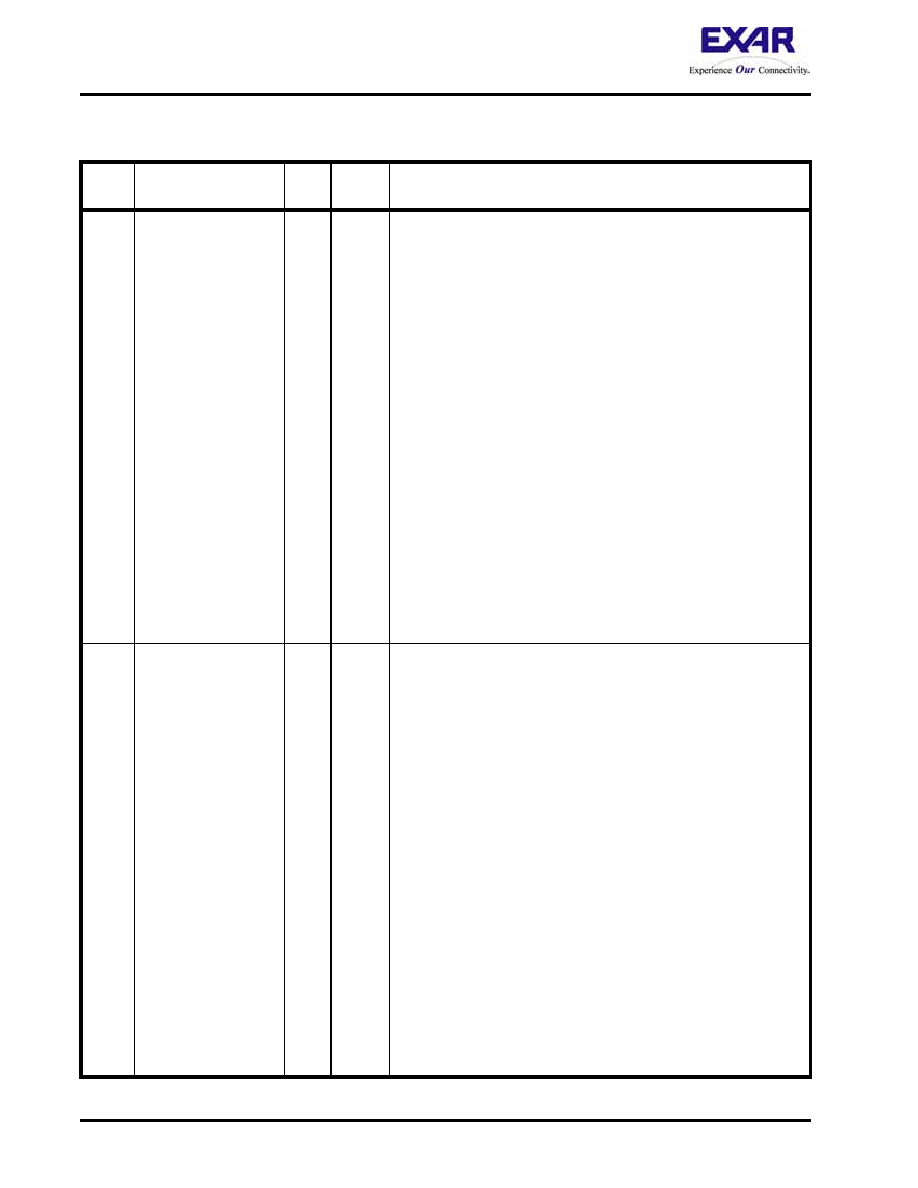
STS-3/STM-1 TELECOM BUS INTERFACE - TRANSMIT DIRECTION
PIN #
SIGNAL NAME
I/O
SIGNAL
TYPE
DESCRIPTION
E15
STS3TxA_CLK_0
TxSBCLK_0
DMO_0
I
TTL
STS-3 Transmit Telecom Bus Clock Input/STM-1 Sub-Rate
Clock/DMO_0 (General Purpose) input Pin:
The function of this input pin depends upon whether or not theSTS-3/
STM-1 Telecom Bus Interface for Channel 0 has been enabled.
If STS-3/STM-1 Telecom Bus (Channel 0) has been enabled -
STS-3 Transmit Telecom Bus Transmit Clock Input - Channel 0:
This input clock signal functions as the clock source for the STS-3/
STM-1 Transmit Telecom Bus, associated with Channel 0. All input
signals (e.g., STS3TxA_ALARM_0, STS3TxA_D_0[7:0],
STS3TxA_DP_0, STS3TxA_PL_0, STS3TxA_C1J1_0) are sampled
upon the falling edge of this input clock signal.
This clock signal should operate at 19.44MHz.
If STS-3/STM-1 Telecom Bus (Channel 0) is disabled - DMO_0
(General Purpose) Input Pin:
This input pin can be used as a general purpose input pin.
The state of this input pin can be determined by reading the state of
Bit 2 (DMO) within the Line Interface Scan Register associated with
Channel 0 (Address = 0x1E, 0x81), (Direct Address = 0x1F81).
NOTE:
For Product Legacy purposes, this pin is called DMO_0,
because one possible application is to tie this input pin to a
DMO (Drive Monitor Output) output pin, from one of Exar's
XRT73L0X/XRT75L0X
DS3/E3/STS-1
LIU
devices.
However, this input pin, and the corresponding register bit
can be used for any purpose.
C26
STS3TxA_CLK_1
TxSBCLK_1
DMO_1
I
TTL
STS-3 Transmit Telecom Bus Clock Input/STM-1 Sub-Rate
Clock/DMO_1 (General Purpose) input Pin:
The function of this input pin depends upon whether or not theSTS-3/
STM-1 Telecom Bus Interface for Channel 1 has been enabled.
If STS-3/STM-1 Telecom Bus (Channel 1) has been enabled -
STS-3 Transmit Telecom Bus Clock Input - Channel 1:
This input clock signal functions as the clock source for the STS-3/
STM-1 Transmit Telecom Bus, associated with Channel 1. All input
signals, (e.g., STS3TxA_ALARM_1, STS3TxA_D_1[7:0],
STS3TxA_DP_1, STS3TxA_PL_1, STS3TxA_C1J1_1) are sampled
upon the falling edge of this input clock signal.
This clock signal should operate at 19.44MHz.
If STS-3/STM-1 Telecom Bus (Channel 1) is disabled - DMO_1
(General Purpose) Input Pin:
This input pin can be used as a general purpose input pin.
The state of this input pin can be determined by reading the state of
Bit 2 (DMO) within the Line Interface Scan Register associated with
Channel 1 (Address = 0x2E, 0x81), (Direct Address = 0x2F81).
NOTE:
For Product Legacy purposes, this pin is called DMO_1
because one possible application is to tie this input pin to a
DMO (Drive Monitor Output) output pin, from one of Exar's
XRT73L0X/XRT75L0X
DS3/E3/STS-1
LIU
devices.
However, this input pin, and the corresponding register bit
can be used for any purpose.
相關(guān)PDF資料 |
PDF描述 |
|---|---|
| VI-B4J-IW-F2 | CONVERTER MOD DC/DC 36V 100W |
| D38999/24FD19SB | CONN RCPT 19POS JAM NUT W/SCKT |
| XRT94L33IB | IC MAPPER DS3/E3/STS-1 504TBGA |
| VI-B4J-IW-F1 | CONVERTER MOD DC/DC 36V 100W |
| 5413558-1 | CONN JACK BNC RT ANG 75 OHM GOLD |
相關(guān)代理商/技術(shù)參數(shù) |
參數(shù)描述 |
|---|---|
| XRT94L43IB-F | 功能描述:網(wǎng)絡(luò)控制器與處理器 IC Demapper RoHS:否 制造商:Micrel 產(chǎn)品:Controller Area Network (CAN) 收發(fā)器數(shù)量: 數(shù)據(jù)速率: 電源電流(最大值):595 mA 最大工作溫度:+ 85 C 安裝風(fēng)格:SMD/SMT 封裝 / 箱體:PBGA-400 封裝:Tray |
| XRT94L55 | 制造商:EXAR 制造商全稱:EXAR 功能描述:SONET/SDH OC-48/STM-16, 4XOC-12/STM-4, 16XOC-3/STM-1 FRAMER/CONCENTRATOR WITH INTEGRATED CDR’S |
| XRT94L55IV | 制造商:EXAR 制造商全稱:EXAR 功能描述:SONET/SDH OC-48/STM-16, 4XOC-12/STM-4, 16XOC-3/STM-1 FRAMER/CONCENTRATOR WITH INTEGRATED CDR’S |
| XRT95L34 | 制造商:EXAR 制造商全稱:EXAR 功能描述:OC-12/STM-4, QUAD OC-3/STM-1 POS/ATM FRAMER WITH INTEGRATED CDR’S |
| XRT95L34IV | 制造商:EXAR 制造商全稱:EXAR 功能描述:OC-12/STM-4, QUAD OC-3/STM-1 POS/ATM FRAMER WITH INTEGRATED CDR’S |
發(fā)布緊急采購,3分鐘左右您將得到回復(fù)。