- 您現(xiàn)在的位置:買賣IC網(wǎng) > PDF目錄372941 > XR17C158CV UART PDF資料下載
參數(shù)資料
| 型號: | XR17C158CV |
| 英文描述: | UART |
| 中文描述: | 異步 |
| 文件頁數(shù): | 18/55頁 |
| 文件大?。?/td> | 734K |
| 代理商: | XR17C158CV |
第1頁第2頁第3頁第4頁第5頁第6頁第7頁第8頁第9頁第10頁第11頁第12頁第13頁第14頁第15頁第16頁第17頁當(dāng)前第18頁第19頁第20頁第21頁第22頁第23頁第24頁第25頁第26頁第27頁第28頁第29頁第30頁第31頁第32頁第33頁第34頁第35頁第36頁第37頁第38頁第39頁第40頁第41頁第42頁第43頁第44頁第45頁第46頁第47頁第48頁第49頁第50頁第51頁第52頁第53頁第54頁第55頁
á
PCI BUS OCTAL UART
XR17C158
REV. 1.1.3
18
MPIOINV [7:0] (default 0x00)
Input inversion control. A logic 0 (default) does not in-
vert the input pin logic. A logic 1 inverts the input logic
level.
MPIOSEL [7:0] (default 0xFF)
Multipurpose input/output pin select. This register de-
fines the functions of the pins. A logic 1 (default) de-
fines the pin for input and a logic "0" for output.
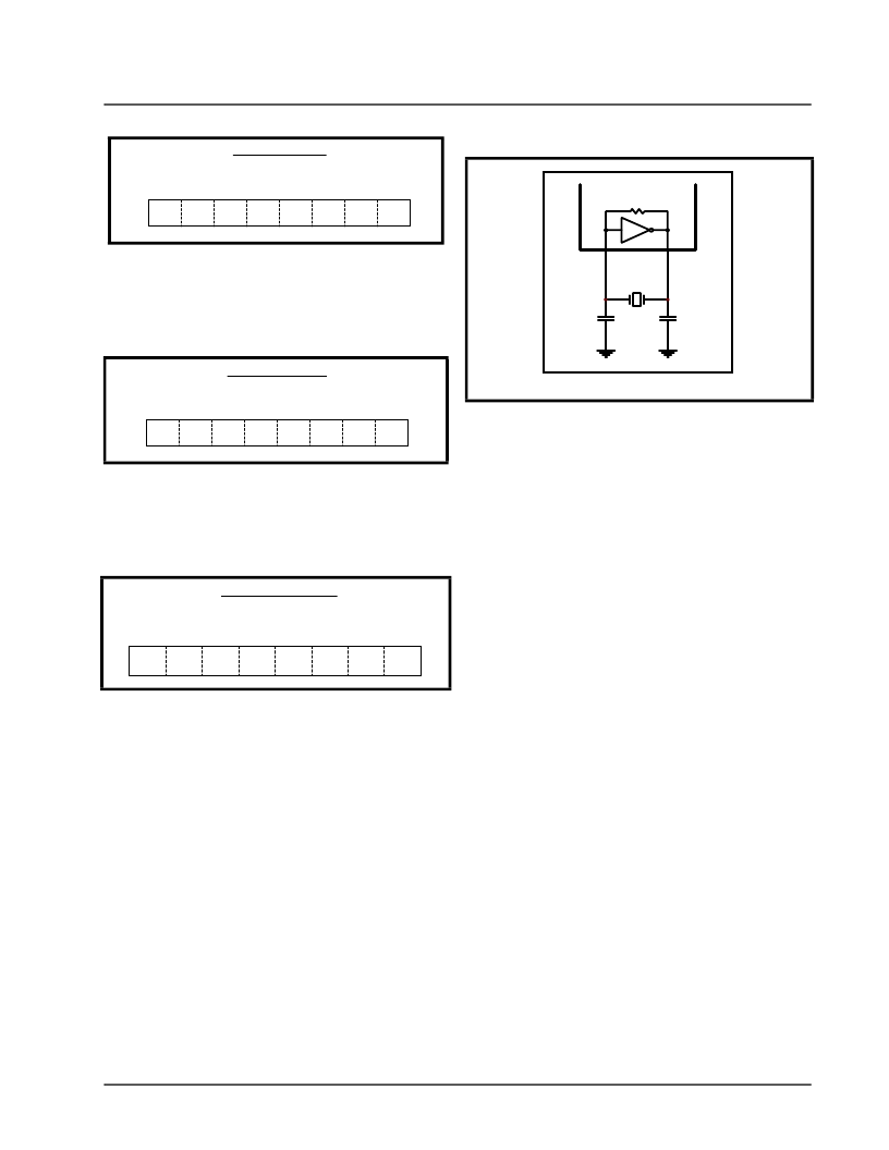
2.0
The 158 includes an on-chip oscillator (XTAL1 and
XTAL2). The crystal oscillator provides the system
clock to the Baud Rate Generators (BRG) in each of
the 8 UARTs, the 16-bit general purpose timer/
counter and internal logics. XTAL1 is the input to the
oscillator or external clock buffer input with XTAL2 pin
being the output. See Programmable Baud Rate
Generator in the UART section for programming de-
tails.
The on-chip oscillator is designed to use an industry
standard microprocessor crystal (parallel resonant
with 10-22 pF capacitance load, 100ppm) connected
externally between the XTAL1 and XTAL2 pins (see
Figure 7
). Alternatively, an external clock can be con-
nected to the XTAL1 pin to clock the internal 8 baud
rate generators for standard or custom rates. Typical-
ly, the oscillator connections are shown in Figure 7.
For further reading on oscillator circuit please see ap-
plication note DAN108 on EXAR’s web site.
CRYSTAL OSCILLATOR / BUFFER
3.0
There are two methods to load transmit data and un-
load receive data from each UART channel. First,
there is a transmit data register and receive data reg-
ister for each UART channel in the device configura-
tion register set to ease programming. These regis-
ters support 8, 16
,
24 and 32 bits wide format. In the
32-bit format, it increases the data transfer rate on the
PCI bus. Additionally, a special register location pro-
vides receive data byte with its associated error flags.
This is a 16-bit or 32-bit read operation where the
Line Status Register (LSR) content in the UART
channel register is paired along with the data byte.
This operation further facilitates data unloading with
the error flags without having to read the LSR register
separately. Furthermore, the XR17C158 supports
PCI burst mode for read/write operation of up to 64
bytes of data.
The second method is through each UART channel’s
transmit holding register (THR) and receive holding
register (RHR). The THR and RHR registers are
16550 compatible so their access is limited to 8-bit
format. The software driver must separately read the
LSR content for the associated error flags before
reading the data byte.
3.1
FIFO
DATA LOADING AND UNLOADING
THROUGH THE DEVICE CONFIGURATION
REGISTERS IN 32-BIT FORMAT.
The transmit and receive data registers are defined
for channel 0 to channel 7 with each channel having
it’s own address as shown in
Table 2
for faster loading
and unloading. The following paragraphs illustrate the
receive and transmit data registers in more detail.
Each Channel Normal Receive Data FIFO
Address
for channels 0 to 7 are at 0x0100, 0x0300, 0x0500,
0x0700, 0x0900, 0x0B000, 0x0D00 and 0x0F00.
TRANSMIT AND RECEIVE DATA
MPIO6
MPIO7
MPIO5 MPIO4 MPIO3 MPIO2 MPIO1 MPIO0
MPIO3T Register
Multipurpose Output 3-state Enable
Bit-7 Bit-6 Bit-5 Bit-4 Bit-3 Bit-2 Bit-1 Bit-0
MPIO6
MPIO7
MPIO5 MPIO4 MPIO3 MPIO2 MPIO1 MPIO0
MPIOINV Register
Multipurpose Input Signal Inversion Enable
Bit-7 Bit-6 Bit-5 Bit-4 Bit-3 Bit-2 Bit-1 Bit-0
MPIO6
MPIO7
MPIO5 MPIO4 MPIO3 MPIO2 MPIO1 MPIO0
MPIOSEL Register
Multipurpose Input/Output Selection
Bit-7 Bit-6 Bit-5 Bit-4 Bit-3 Bit-2 Bit-1 Bit-0
F
IGURE
7. T
YPICAL
OSCILLATOR
CONNECTIONS
C1
22-47pF
C2
22-47pF
14.7456
MHz
XTAL1
XTAL2
R=300K to 400K
相關(guān)PDF資料 |
PDF描述 |
|---|---|
| XR17C158IV | UART |
| XR215CP | IC-PHASE LOCKED LOOP |
| XR215 | Monolithic Phase Locked Loop |
| XR2206CP | IC-FUNCTION GENERATOR |
| XR2207MD | Waveform Generator/Support |
相關(guān)代理商/技術(shù)參數(shù) |
參數(shù)描述 |
|---|---|
| XR17C158CV-0A-EVB | 功能描述:UART 接口集成電路 Supports C158 144 ld TQFP, PCI Interface RoHS:否 制造商:Texas Instruments 通道數(shù)量:2 數(shù)據(jù)速率:3 Mbps 電源電壓-最大:3.6 V 電源電壓-最小:2.7 V 電源電流:20 mA 最大工作溫度:+ 85 C 最小工作溫度:- 40 C 封裝 / 箱體:LQFP-48 封裝:Reel |
| XR17C158CV-F | 功能描述:UART 接口集成電路 UART RoHS:否 制造商:Texas Instruments 通道數(shù)量:2 數(shù)據(jù)速率:3 Mbps 電源電壓-最大:3.6 V 電源電壓-最小:2.7 V 電源電流:20 mA 最大工作溫度:+ 85 C 最小工作溫度:- 40 C 封裝 / 箱體:LQFP-48 封裝:Reel |
| XR17C158CVTR-F | 制造商:Exar Corporation 功能描述:UART 8-CH 64Byte FIFO 5V 144-Pin LQFP T/R 制造商:Exar Corporation 功能描述:XR17C158CVTR-F |
| XR17C158IV | 功能描述:UART 接口集成電路 UART RoHS:否 制造商:Texas Instruments 通道數(shù)量:2 數(shù)據(jù)速率:3 Mbps 電源電壓-最大:3.6 V 電源電壓-最小:2.7 V 電源電流:20 mA 最大工作溫度:+ 85 C 最小工作溫度:- 40 C 封裝 / 箱體:LQFP-48 封裝:Reel |
| XR17C158IV-F | 功能描述:UART 接口集成電路 UART RoHS:否 制造商:Texas Instruments 通道數(shù)量:2 數(shù)據(jù)速率:3 Mbps 電源電壓-最大:3.6 V 電源電壓-最小:2.7 V 電源電流:20 mA 最大工作溫度:+ 85 C 最小工作溫度:- 40 C 封裝 / 箱體:LQFP-48 封裝:Reel |
發(fā)布緊急采購,3分鐘左右您將得到回復(fù)。