- 您現(xiàn)在的位置:買賣IC網(wǎng) > PDF目錄384039 > UPC1862 (NEC Corp.) BURST LOCK CLOCK GENERATOR PDF資料下載
參數(shù)資料
| 型號(hào): | UPC1862 |
| 廠商: | NEC Corp. |
| 英文描述: | BURST LOCK CLOCK GENERATOR |
| 中文描述: | 爆破鎖時(shí)鐘發(fā)生器 |
| 文件頁數(shù): | 21/32頁 |
| 文件大小: | 252K |
| 代理商: | UPC1862 |
第1頁第2頁第3頁第4頁第5頁第6頁第7頁第8頁第9頁第10頁第11頁第12頁第13頁第14頁第15頁第16頁第17頁第18頁第19頁第20頁當(dāng)前第21頁第22頁第23頁第24頁第25頁第26頁第27頁第28頁第29頁第30頁第31頁第32頁
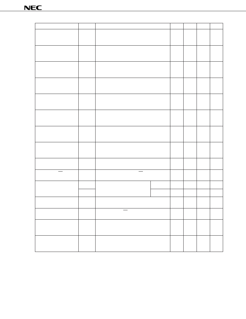
21
μ
PC1862
Parameter
Symbol
Condition
MIN.
TYP.
MAX.
Unit
Field ident. output
High level (1)
E
FIOH1
High level of synchronized Field ident. output
when only 0.3 V
p-p
sync signal is input to pin 36
I
OH
= –400
μ
A
2.7
3.8
-
V
Field ident. output
High level (2)
E
FIOH2
High level of synchronized Field ident. output
when only 0.3 V
p-p
sync signal is input to pin 36
I
OH
= –20
μ
A
3.5
4.3
-
V
Field idnet. output
Low level
E
FIOL
High level of synchronized Field ident. output
when only 0.3 V
p-p
sync signal is input to pin 36
I
OL
= +2 mA
-
0.1
0.4
V
H detection output
High level (1)
E
FIOH1
High level of asynchronized H detect output
without H sync input
I
OH
= –400
μ
A
2.7
3.8
-
V
H detection output
High level (2)
E
FIOH2
High level of asynchronized H detect output
without H sync input
I
OH
= –20
μ
A
3.5
4.3
-
V
H detection output
Low level
E
FIOL
High level of synchronized H detect output
when only 0.3 V
p-p
sync signal is input to pin 36
I
OL
= +2 mA
-
0.1
0.4
V
H sync lock-in range
f
HP
Frequency range that can be pulled when only
0.3 V
p-p
sync signal is input to pin 36 and H
sync frequency is varied (f
SC
conversion)
±
400
±
500
-
Hz
Horizontal VCO control
sensitivity
β
H
Rate of variation of frequency when APC filter
pin is changed form 3.0 V to 3.4 V without H
sync input (f
SC
conversion)
–1.6
–1.3
–0.9
Hz/mV
Horizontal VCO free-run
frequency
f
HO
Frequency difference of HD output from f
H
when H sync input is not applied
–100
–25
+50
Hz
Pulse width of HD output
P
WNHSO
Pulse width of synchronized HD output when
only 0.3 V
p-p
sync signal is input to pin 36
3.8
4.0
4.2
μ
s
Pulse width of VD output
P
WVSO1
Pulse width of synchronized VD
output when only 0.3 V
p-p
sync
signal is input to pin 36
ODD
-
6.0
-
H
Note
P
WVSO2
EVEN
-
5.5
-
H
Note
Pulse width of Clamp output
P
WCPO
Pulse width of synchronized Clamp output when
only 0.3 V
p-p
sync signal is input to pin 36
3.4
3.6
3.8
μ
s
Oscillation start voltage of
horizontal VCO
V
ST
Output voltage at HD when V
CC
is gradually
increased from 0 V without H sync input
-
-
4.2
V
H killer output Low level
E
HKOL
Low level of synchronized H killer output when
only 0.3 V
p-p
sync signal is input to pin 36
Change value of Chroma output
-
-
0.4
V
Burst gate input
Threshold level 1
V
BGPE1
Burst gate pulse input voltage when Clamp
voltage begins Low level is gradually increased
from 0 V without signal input
1.6
1.9
2.0
V
Note
H: Horizontal scanning period
相關(guān)PDF資料 |
PDF描述 |
|---|---|
| UPC1862GS | BURST LOCK CLOCK GENERATOR |
| UPC1883 | BIPOLAR ANALOG INTEGRATED CIRCUIT |
| UPC1909 | Isolated Flyback Switching Regulator with 9V Output |
| UPC1909CX | Isolated Flyback Switching Regulator with 9V Output |
| UPC1909GS | Isolated Flyback Switching Regulator with 9V Output |
相關(guān)代理商/技術(shù)參數(shù) |
參數(shù)描述 |
|---|---|
| UPC1862GS | 制造商:NEC 制造商全稱:NEC 功能描述:BURST LOCK CLOCK GENERATOR |
| UPC1870CA001 | 制造商:Panasonic Industrial Company 功能描述:IC |
| UPC1872CU | 制造商:NEC 制造商全稱:NEC 功能描述:US MTS DECODER |
| UPC1872GH | 制造商:Panasonic Industrial Company 功能描述:IC |
| UPC1874CT | 制造商:未知廠家 制造商全稱:未知廠家 功能描述:TV/Video Sound Circuit |
發(fā)布緊急采購,3分鐘左右您將得到回復(fù)。