- 您現(xiàn)在的位置:買賣IC網(wǎng) > PDF目錄383967 > TUA6100B6 (INFINEON TECHNOLOGIES AG) Components for Satellite Receiver Units PDF資料下載
參數(shù)資料
| 型號(hào): | TUA6100B6 |
| 廠商: | INFINEON TECHNOLOGIES AG |
| 英文描述: | Components for Satellite Receiver Units |
| 中文描述: | 元件衛(wèi)星接收單元 |
| 文件頁(yè)數(shù): | 31/46頁(yè) |
| 文件大小: | 819K |
| 代理商: | TUA6100B6 |
第1頁(yè)第2頁(yè)第3頁(yè)第4頁(yè)第5頁(yè)第6頁(yè)第7頁(yè)第8頁(yè)第9頁(yè)第10頁(yè)第11頁(yè)第12頁(yè)第13頁(yè)第14頁(yè)第15頁(yè)第16頁(yè)第17頁(yè)第18頁(yè)第19頁(yè)第20頁(yè)第21頁(yè)第22頁(yè)第23頁(yè)第24頁(yè)第25頁(yè)第26頁(yè)第27頁(yè)第28頁(yè)第29頁(yè)第30頁(yè)當(dāng)前第31頁(yè)第32頁(yè)第33頁(yè)第34頁(yè)第35頁(yè)第36頁(yè)第37頁(yè)第38頁(yè)第39頁(yè)第40頁(yè)第41頁(yè)第42頁(yè)第43頁(yè)第44頁(yè)第45頁(yè)第46頁(yè)
Preliminary Specification
TUA6100B6
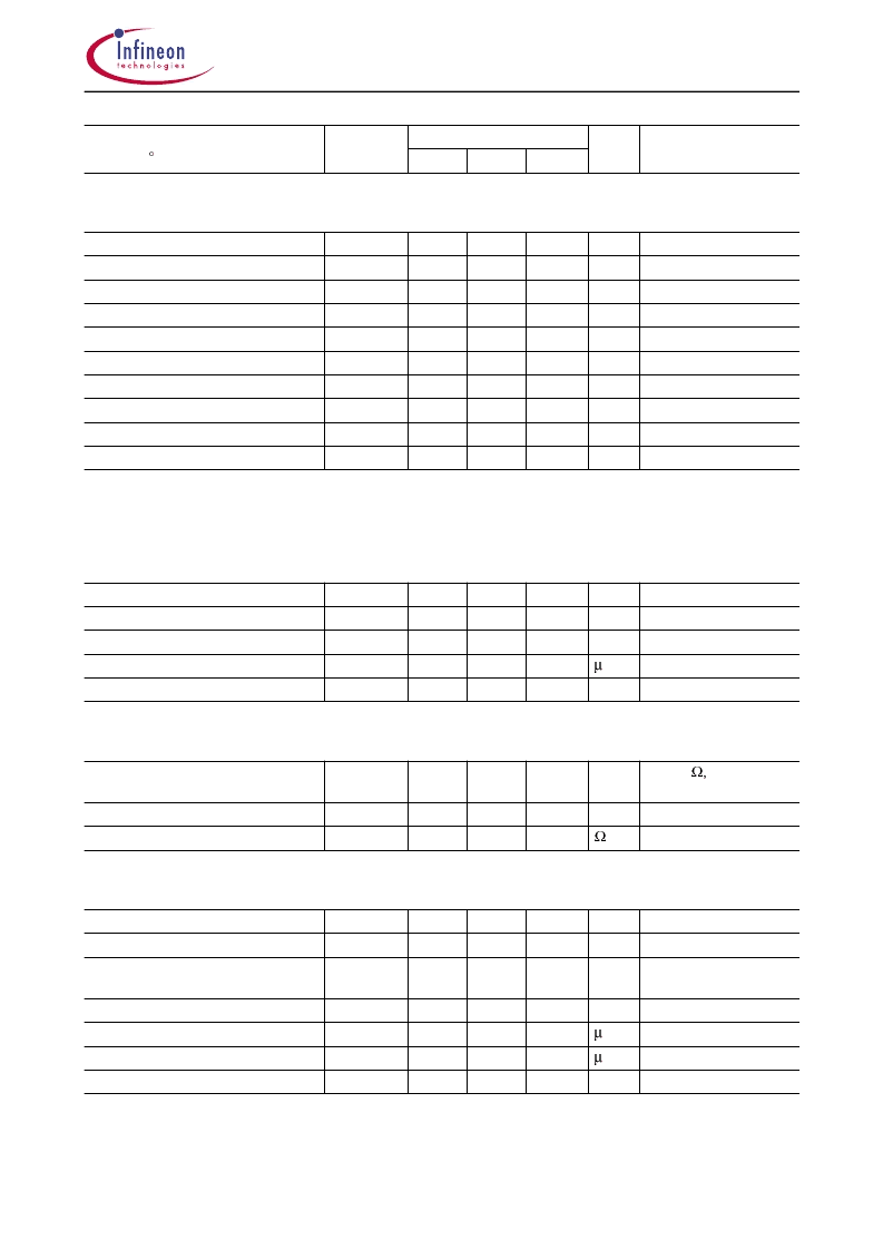
High-Frequency-Products
26
26.1.01
Synthesizer VCO
(
see Synthesizer VCO on page 6
)
DC voltage
high side VCO frequency range
high side VCO frequency range
low side VCO frequency range
low side VCO frequency range
high side VCO frequency range
low side VCO frequency range
Phase noise high side VCO
1)
Phase noise high side VCO
1)
Phase noise high side VCO
1)
1)
Note : This is the phase noise of the free running VCO, not for the overall system performance at
baseband output. For detailed system phase noise information see diagrams
page 30
and
page 31
and
our separate application note.
V
OB1
,V
OB2
f
VCO
f
VCO
f
VCO
f
VCO
f
VCO
f
VCO
1.9
V
MHz
MHz
MHz
MHz
MHz
MHz
dBc
dBc
dBc
1900
1900
712
700
1424
950
- 53
- 73
- 93
2870
2910
1076
1075
2151
1434
- 60
- 80
- 100
2 band split,
page 32
3 band split,
page 32
2 band split,
page 32
3 band split,
page 32
+VCO at f
in
, band split
+VCO at f
in
, band split
1 kHz offset, SSB
10 kHz offset, SSB
100 kHz offset, SSB
- 56
- 76
- 96
Port outputs, P0, P1, P2
(
see Output Ports on page 5
)
Supply voltage
LOW output voltage
LOW output current
HIGH output current
Port outputs, I=max
V
P
V
P
I
P
I
P
t
Imax
0
0
5.5
0.5
15
10
1
V
V
mA
A
ms
max. Vcc
I
P
= 15 mA
0
V
P
= 5 V
V
P0,P1,P2
=V
VCC
Crystal oscillator output
(
see Crystal Oscillator Output on page 6
)
Buffer output voltage
1)
V
Xtalout
1.1
V
pp
R
L
>1M
C
L
= 10 pF, f = 16 MHz
Vcc=5V,
Buffer output current
Buffer output impedance
I
Xtalout
R
Xtalout
1
mA
350
I
2
C and 3-Wire-bus
Clock, Data, Enable, BUS_MODE (see
Bus Data Format on page 16
and
8.13.5 Bus Timing on page 19
)
HIGH level input voltage
V
IH
2.24
LOW level input voltage
V
IL
-0.5
LOW level output voltage
(DATA), only I2C-bus
Hysteresis of Schmitt trigger inputs V
hys
0.2
H-input current
I
H
L-input current
I
L
-60
Input capacity
C
I
V
VCC
0.96
0.4
0.6
V
V
V
OL
0
V
3mA sink current
6mA sink current
1
V
10
A
A
V
I
= V
VCC
= 5.5V
V
I
= GND
5
pF
1) output voltage is dependant on Vcc
Parameter
T
A
= 25 C,V
VCC
, V
VCC1
= 5V
Symbol
Limit Values
typ
Unit
Test conditions
min
max
相關(guān)PDF資料 |
PDF描述 |
|---|---|
| TV06B5V0K-G | SMD TRANSLENT VOLTAGE SUPPRESSOR |
| TV06B6V0J-G | SMD TRANSLENT VOLTAGE SUPPRESSOR |
| TV06B6V0K-G | SMD TRANSLENT VOLTAGE SUPPRESSOR |
| TV06B7V0J-G | SMD TRANSLENT VOLTAGE SUPPRESSOR |
| TV06B7V0K-G | SMD TRANSLENT VOLTAGE SUPPRESSOR |
相關(guān)代理商/技術(shù)參數(shù) |
參數(shù)描述 |
|---|---|
| TUA6110XS | 制造商:未知廠家 制造商全稱:未知廠家 功能描述:RF Mixer |
| TUA6120 | 制造商:INFINEON 制造商全稱:Infineon Technologies AG 功能描述:Gain controlled I/Q Mixer for Digital QPSK or 8PSK Sat Signals |
| TUA9001XT | 制造商:Infineon Technologies AG 功能描述:Tuners 38.4MHz 65-Pin WFSGA |
| TUB-1.25(100pcs) | 制造商:JST Manufacturing 功能描述:_ 3.4mm 0.25 to 1.65mm2 Bulk |
| TUB-120-AKA-010 | 制造商:ATC DIVERSIFIED ELECTRONICS 功能描述:RELAY;TIME DLY RLY INTER.ON OPT RLY OTPT |
發(fā)布緊急采購(gòu),3分鐘左右您將得到回復(fù)。