- 您現(xiàn)在的位置:買賣IC網(wǎng) > PDF目錄383967 > TUA6100B6 (INFINEON TECHNOLOGIES AG) Components for Satellite Receiver Units PDF資料下載
參數(shù)資料
| 型號(hào): | TUA6100B6 |
| 廠商: | INFINEON TECHNOLOGIES AG |
| 英文描述: | Components for Satellite Receiver Units |
| 中文描述: | 元件衛(wèi)星接收單元 |
| 文件頁數(shù): | 23/46頁 |
| 文件大?。?/td> | 819K |
| 代理商: | TUA6100B6 |
第1頁第2頁第3頁第4頁第5頁第6頁第7頁第8頁第9頁第10頁第11頁第12頁第13頁第14頁第15頁第16頁第17頁第18頁第19頁第20頁第21頁第22頁當(dāng)前第23頁第24頁第25頁第26頁第27頁第28頁第29頁第30頁第31頁第32頁第33頁第34頁第35頁第36頁第37頁第38頁第39頁第40頁第41頁第42頁第43頁第44頁第45頁第46頁
Preliminary Specification
TUA6100B6
High-Frequency-Products
18
26.1.01
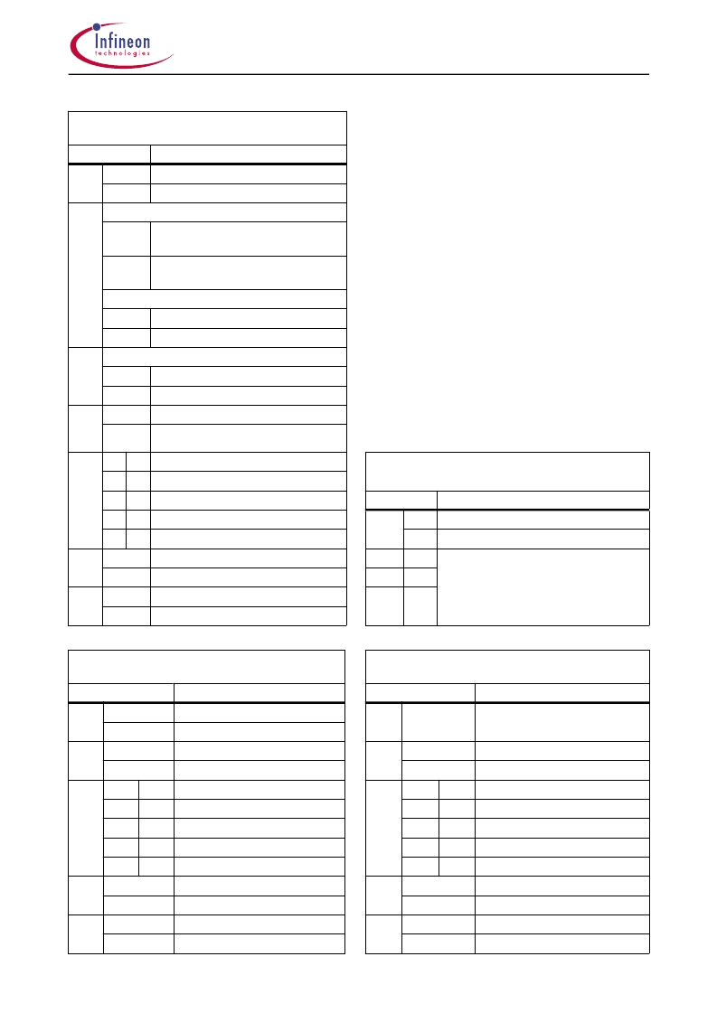
Control-Register
(Register 00) ---> Subaddress 00H
Bit
0
Normal-Mode
1
Test-Mode
D7 must be = 1 (Test-Mode)
R-counter / 2 -> output to Port P0
N-counter / 2 -> output to Port P1
Port P0 -> input to R-counter
Port P1 -> input to N-counter
D7 must be = 0 (Normal-Mode)
0
Bit D5 not active
1
Bit D5 active
D5 is only active for D6 = 1, D7 = 0
0
LockDetect output on Port 0
1
LockDetect output on Port 2
0
PhaseDetector polarity negative
Test-Mode:
It is possible to switch into an internal chip test mode
by bit D7 of the control register (subaddress 00H).
If test mode is activated there are two test options
available by bit D6 of the control register:
D6 = 0 --> Test-Mode1:
In this case the output frequencies of the
counters divided by 2 ( ! ) are put out to the
Ports P0 ( R-counter output frequency / 2 )
and P1 ( N-counter output frequency / 2 )
Nevertheless the phase detector and the
charge pump are in function
( lock detector = OFF ).
D6 = 1 --> Test-Mode2:
In this case the phase detector, charge pump
and lock detector (= ON) can be tested by
external frequencies which are applied to the
Ports P0 (path of the R-counter frequency)
and P1 (path of the N-counter frequency).
( Note: LD_out only on port P2 visible! )
Function
MSB
D7
D6
0
1
D5
D4
1
PhaseDetector polarity positive
D3
D2
D3 D2 Synthesizer ChargePump current
0
0
100μA
0
1
500μA
1
0
1mA
1
1
2mA
0
Synthesizer ChargePump disabled
1
Synthesizer ChargePump enabled
0
Synthesizer Loopfilter OP disabled
1
Synthesizer Loopfilter OP enabled
Status-Register (READ)
(Register 128) ---> Subaddress 80H
Bit
Function
MSB
D7
0
1
1
1
synthesizer PLL unlocked
synthesizer PLL locked
D1
D6
.....
for future use, all bits = 1
D0
LSB
D0
LSB
1
Prescaler, Ports, GHz-PLL
(Register 01) ---> Subaddress 01H
Bit
0
GHz VCO = 3.4-6.2 GHz
1
GHz VCO = 6-8.6 GHz
0
Prescaler divide ratio 32/33
1
Prescaler divide ratio 64/65
D21
D20
N-Counter GHz-PLL
0
0
0
1
1
0
1
1
0
Port_1 output = low level
1
Port_1 output = high level
0
Port_0 output = low level
1
Port_0 output = high level
Ports, GHz-PLL
(Register 02) ---> Subaddress 02H
Bit
Function
Function
MSB
D23
MSB
D15
0
not used (must be=0)
D22
D14
0
1
base band amplifier enabled
base band amplifier disabled
R-Counter GHz-PLL
D21
D20
D13
D12
D13
0
0
1
1
D12
0
1
0
1
: 3
: 4
: 2
: 3
: 3
: 4
: 2
: 3
D19
D11
0
1
0
1
-
-
Port_2 output = low level
Port_2 output = high level
D18
D10
相關(guān)PDF資料 |
PDF描述 |
|---|---|
| TV06B5V0K-G | SMD TRANSLENT VOLTAGE SUPPRESSOR |
| TV06B6V0J-G | SMD TRANSLENT VOLTAGE SUPPRESSOR |
| TV06B6V0K-G | SMD TRANSLENT VOLTAGE SUPPRESSOR |
| TV06B7V0J-G | SMD TRANSLENT VOLTAGE SUPPRESSOR |
| TV06B7V0K-G | SMD TRANSLENT VOLTAGE SUPPRESSOR |
相關(guān)代理商/技術(shù)參數(shù) |
參數(shù)描述 |
|---|---|
| TUA6110XS | 制造商:未知廠家 制造商全稱:未知廠家 功能描述:RF Mixer |
| TUA6120 | 制造商:INFINEON 制造商全稱:Infineon Technologies AG 功能描述:Gain controlled I/Q Mixer for Digital QPSK or 8PSK Sat Signals |
| TUA9001XT | 制造商:Infineon Technologies AG 功能描述:Tuners 38.4MHz 65-Pin WFSGA |
| TUB-1.25(100pcs) | 制造商:JST Manufacturing 功能描述:_ 3.4mm 0.25 to 1.65mm2 Bulk |
| TUB-120-AKA-010 | 制造商:ATC DIVERSIFIED ELECTRONICS 功能描述:RELAY;TIME DLY RLY INTER.ON OPT RLY OTPT |
發(fā)布緊急采購,3分鐘左右您將得到回復(fù)。