- 您現(xiàn)在的位置:買(mǎi)賣(mài)IC網(wǎng) > PDF目錄98301 > TSC2003IR (TEXAS INSTRUMENTS INC) 3-CH 12-BIT SUCCESSIVE APPROXIMATION ADC, SERIAL ACCESS, PDSO16 PDF資料下載
參數(shù)資料
| 型號(hào): | TSC2003IR |
| 廠商: | TEXAS INSTRUMENTS INC |
| 元件分類: | ADC |
| 英文描述: | 3-CH 12-BIT SUCCESSIVE APPROXIMATION ADC, SERIAL ACCESS, PDSO16 |
| 封裝: | PLASTIC, TSSOP-16 |
| 文件頁(yè)數(shù): | 9/20頁(yè) |
| 文件大小: | 309K |
| 代理商: | TSC2003IR |
第1頁(yè)第2頁(yè)第3頁(yè)第4頁(yè)第5頁(yè)第6頁(yè)第7頁(yè)第8頁(yè)當(dāng)前第9頁(yè)第10頁(yè)第11頁(yè)第12頁(yè)第13頁(yè)第14頁(yè)第15頁(yè)第16頁(yè)第17頁(yè)第18頁(yè)第19頁(yè)第20頁(yè)

TSC2003
17
SBAS162A
www.ti.com
I2C High-Speed Operation
The TSC2003 can operate with high-speed I2C masters. To
do so, the simple resistor pullup on SCL must be changed to
the active pull-up, as recommended in the I2C specification.
The I2C bus will be operating in standard or fast mode
initially. Following a START condition, the master will
send the code 00001xxx, which the slave will not acknowl-
edge. At this point, the bus is now operating in high-speed
mode. The bus will remain in high-speed mode until a STOP
condition occurs. Therefore, to maximize throughput only
repeated STARTs should be used to separate transactions.
Since the TSC2003 may not have completed a conversion
before a read to the part can be requested, the TSC2003 is
capable of stretching the clock until the converted data is
stored in its internal shift register. Once the data is latched,
the TSC2003 will release the clock line so that the master
can receive the converted data. A complete high-speed
Conversion Cycle is shown in Figure 14.
Data Format
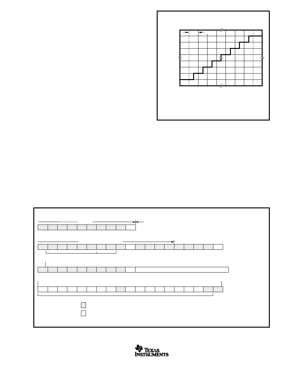
The TSC2003 output data is in Straight Binary format, as
shown in Figure 15. This shows the ideal output code for the
given input voltage, and does not include the effects of
offset, gain, or noise.
8-Bit Conversion
The TSC2003 provides an 8-bit conversion mode (M = 1)
that can be used when faster throughput is needed, and the
digital result is not as critical (for example, measuring
pressure). By switching to the 8-bit mode, a conversion
result can be read by transferring only one data byte.
This shortens each conversion by four bits and reduces data
transfer time which results in fewer clock cycles and pro-
vides lower power consumption.
D11
D10
D9
D8
D7
D6
D5
D4
A
D3
D0
N
P
S
0
1
X
Sr
1
0
1
0
A1
A0
W
A
C3
C2
C1
C0
PD1
PD0
M
X
A
Sr
1
0
1
0
A1
A0
R
A
SCLH is stretched LOW until A/D Converter is finished converting data.
N
D2
D1
00
0
F/S Mode
HS-Mode Enabled
A/D Converter Power-Down Mode
A/D Converter Powers Up and Begins Sampling
Fixed Address Part
Programmable
A/D Converter Stops Sampling and Begins Conversion Using Internal Clock
A/D Converter Goes Into Power-Down Mode After Finishing Conversion (If PD0 = 0)
Exit HS-Mode and Enter F/S Mode
16 Bits + Ack
S = START
Sr = REPEATED START
P = STOP
= Master Controls Bus
= Slave Controls Bus
FIGURE 14. High-Speed I2C Mode Conversion Cycle.
Output
Code
0V
FS = Full-Scale Voltage = V
REF
(1)
1LSB = V
REF
(1)/4096
FS – 1LSB
11...111
11...110
11...101
00...010
00...001
00...000
1LSB
NOTES: (1) Reference voltage at converter: +REF – (–REF). See Figure 2.
(2) Input voltage at converter, after multiplexer: +IN – (–IN). See Figure 2
Input Voltage(2) (V)
FIGURE 15. Ideal Input Voltages and Output Codes.
LAYOUT
The following layout suggestions should provide optimum
performance from the TSC2003. However, many portable
applications have conflicting requirements concerning power,
cost, size, and weight. In general, most portable devices have
fairly “clean” power and grounds because most of the internal
components are very low power. This situation would mean
less bypassing for the converter's power, and less concern
regarding grounding. Still, each situation is unique, and the
following suggestions should be reviewed carefully.
相關(guān)PDF資料 |
PDF描述 |
|---|---|
| TSC2008IRGVR | SPECIALTY CONSUMER CIRCUIT, PQCC16 |
| TSC2008IRGVT | SPECIALTY CONSUMER CIRCUIT, PQCC16 |
| TSC2008IYZGR | SPECIALTY CONSUMER CIRCUIT, BGA12 |
| TSC2008IYZGT | SPECIALTY CONSUMER CIRCUIT, BGA12 |
| TSC2008TRGVRQ1 | SPECIALTY CONSUMER CIRCUIT, PQCC16 |
相關(guān)代理商/技術(shù)參數(shù) |
參數(shù)描述 |
|---|---|
| TSC2003IZQCR | 功能描述:觸摸屏轉(zhuǎn)換器和控制器 4-wire Touch Screen Controller RoHS:否 制造商:Microchip Technology 類型:Resistive Touch Controllers 輸入類型:3 Key 數(shù)據(jù)速率:140 SPS 分辨率:10 bit 接口類型:4-Wire, 5-Wire, 8-Wire, I2C, SPI 電源電壓:2.5 V to 5.25 V 電源電流:17 mA 工作溫度:- 40 C to + 85 C 封裝 / 箱體:SSOP-20 |
| TSC2003-Q1 | 制造商:TI 制造商全稱:Texas Instruments 功能描述:I2C TOUCH SCREEN CONTROLLER |
| TSC2004 | 制造商:BB 制造商全稱:BB 功能描述:1.2V to 3.6V, 12-Bit, Nanopower, 4-Wire TOUCH SCREEN CONTROLLER with I2C⑩ Interface |
| TSC2004_12 | 制造商:BB 制造商全稱:BB 功能描述:1.2V to 3.6V, 12-Bit, Nanopower, 4-Wire |
| TSC2004EVM | 功能描述:觸摸傳感器開(kāi)發(fā)工具 TSC2004EVM Eval Mod RoHS:否 制造商:Cypress Semiconductor 工具用于評(píng)估: 接口類型: 工作電壓: 最大工作溫度: |
發(fā)布緊急采購(gòu),3分鐘左右您將得到回復(fù)。