- 您現(xiàn)在的位置:買賣IC網 > PDF目錄199479 > TSB43AA82GGW (TEXAS INSTRUMENTS INC) 2 CHANNEL(S), 400M bps, SERIAL COMM CONTROLLER, PBGA176 PDF資料下載
參數資料
| 型號: | TSB43AA82GGW |
| 廠商: | TEXAS INSTRUMENTS INC |
| 元件分類: | 微控制器/微處理器 |
| 英文描述: | 2 CHANNEL(S), 400M bps, SERIAL COMM CONTROLLER, PBGA176 |
| 封裝: | PLASTIC, BGA-176 |
| 文件頁數: | 39/146頁 |
| 文件大小: | 770K |
| 代理商: | TSB43AA82GGW |
第1頁第2頁第3頁第4頁第5頁第6頁第7頁第8頁第9頁第10頁第11頁第12頁第13頁第14頁第15頁第16頁第17頁第18頁第19頁第20頁第21頁第22頁第23頁第24頁第25頁第26頁第27頁第28頁第29頁第30頁第31頁第32頁第33頁第34頁第35頁第36頁第37頁第38頁當前第39頁第40頁第41頁第42頁第43頁第44頁第45頁第46頁第47頁第48頁第49頁第50頁第51頁第52頁第53頁第54頁第55頁第56頁第57頁第58頁第59頁第60頁第61頁第62頁第63頁第64頁第65頁第66頁第67頁第68頁第69頁第70頁第71頁第72頁第73頁第74頁第75頁第76頁第77頁第78頁第79頁第80頁第81頁第82頁第83頁第84頁第85頁第86頁第87頁第88頁第89頁第90頁第91頁第92頁第93頁第94頁第95頁第96頁第97頁第98頁第99頁第100頁第101頁第102頁第103頁第104頁第105頁第106頁第107頁第108頁第109頁第110頁第111頁第112頁第113頁第114頁第115頁第116頁第117頁第118頁第119頁第120頁第121頁第122頁第123頁第124頁第125頁第126頁第127頁第128頁第129頁第130頁第131頁第132頁第133頁第134頁第135頁第136頁第137頁第138頁第139頁第140頁第141頁第142頁第143頁第144頁第145頁第146頁
123
4.
Load capacitance: For parallel resonant mode crystal circuits, the frequency of oscillation is dependent
upon the load capacitance specified for the crystal. Total load capacitance (CL) is a function of not only the
discrete load capacitors, but also board layout and circuit. It is recommended that load capacitors with a
maximum of
±5% tolerance be used.
As an example, for the TSB43AA82 evaluation module (EVM) which uses a crystal specified for 20 pF loading, load
capacitors (C9 and C10 in Figure 124) of 27 pF each were appropriate for the layout of that particular board. The
load specified for the crystal includes the load capacitors (C9, C10), the loading of the PHY pins (CPHY), and the
loading of the board itself (CBD). The value of CPHY is typically about 1 pF, and CBD is typically 0.8 pF per centimeter
of board etch; a typical board can have 3 pF to 6 pF or more. The load capacitors C9 and C10 combine as capacitors
in series so that the total load capacitance is:
C
L +
(C9
C10)
C9
) C10 )
C
PHY )
C
BD
XO
C9
C10
24.576 MHz
X1
C
PHY
+ C
BD
XI
Is
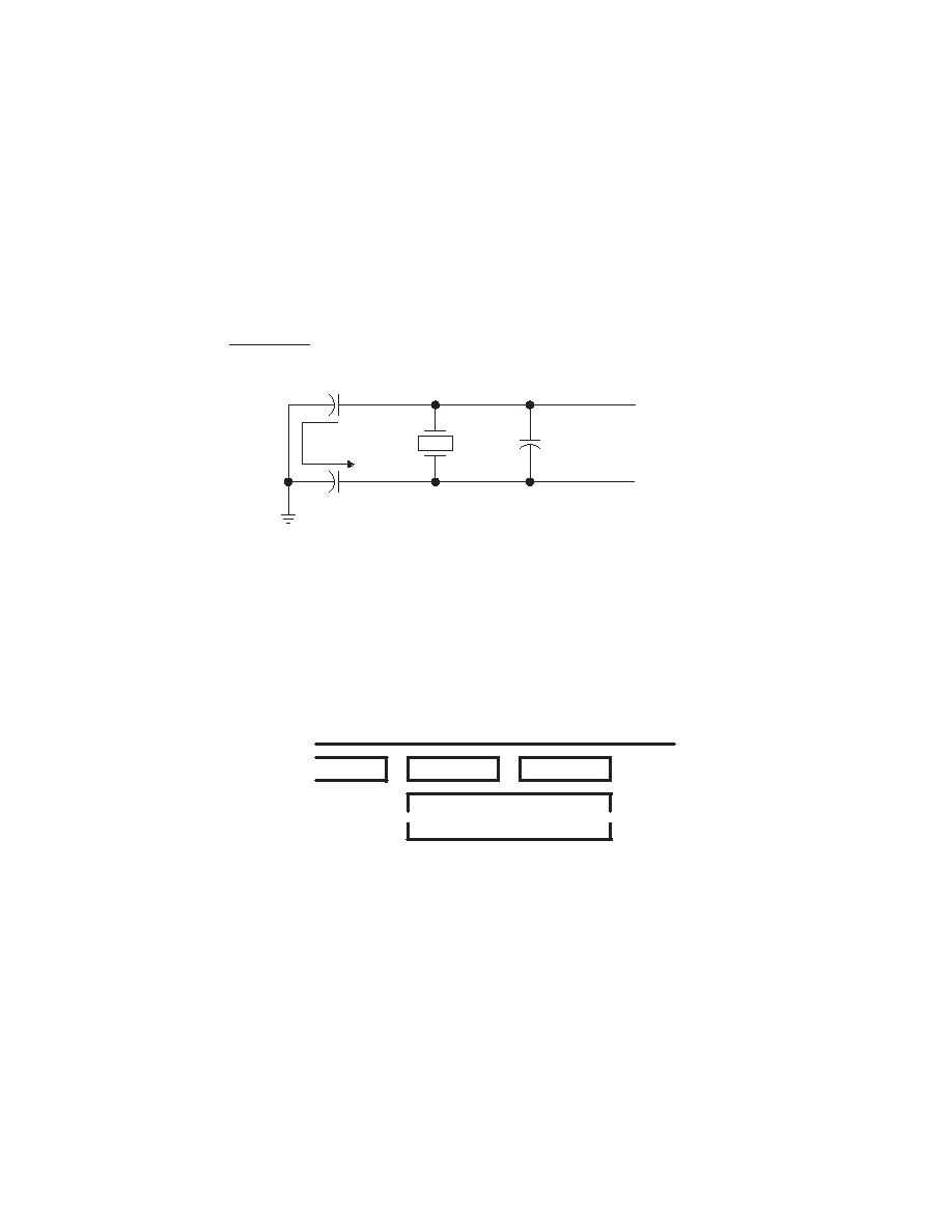
Figure 124. Load Capacitance for the TSB43AA82 PHY Portion
NOTE: The layout of the crystal portion of the PHY circuit is important for obtaining the correct
frequency, minimizing noise introduced into the PHY’s phase-lock loop, and minimizing any
emissions from the circuit. The crystal and two load capacitors should be considered as a unit
during layout. The crystal and load capacitors should be placed as close as possible to one
another while minimizing the loop area created by the combination of the three components.
Varying the size of the capacitors may help in this. Minimizing the loop area minimizes the effect
of the resonant current (Is) that flows in this resonant circuit. This layout unit (crystal and load
capacitors) should then be placed as close as possible to the PHY XI and XO pins to minimize
trace lengths.
C9
C10
X1
Figure 125. Recommended Crystal and Capacitor Layout
12.3 Bus Reset
In the TSB43AA82, the initiate bus reset (IBR) bit can be set to 1 in order to initiate a bus reset and initialization
sequence. The IBR bit is located in PHY register 1, along with the root-holdoff bit (RHB) and Gap_Count field, as
required by the P1394a supplement (this configuration also maintains compatibility with older TI PHY designs which
were based upon the suggested register set defined in Annex J of IEEE Std 1394-19951). Therefore, whenever the
IBR bit is written, the RHB bit and Gap_Count field are also necessarily written.
The RHB bit and gap-count may also be updated by PHY-config packets. The TSB43AA82 is P1394a compliant, and
therefore both the reception and transmission of PHY-config packets cause the RHB and gap-count to be loaded,
unlike older IEEE Std 1394-1995 compliant PHYs which decode only received PHY-config packets.
1 IEEE Std 1394-1995, IEEE Standard for a High Performance Serial Bus
相關PDF資料 |
PDF描述 |
|---|---|
| TSB43DA42GHCR | PCI BUS CONTROLLER, PBGA196 |
| TSB500SK02 | 30 A, BARRIER STRIP TERMINAL BLOCK, 1 ROW, 1 DECK |
| TSB500SK10MDS | 30 A, BARRIER STRIP TERMINAL BLOCK, 1 ROW, 1 DECK |
| TSB5000331DS | 30 A, BARRIER STRIP TERMINAL BLOCK, 1 ROW, 1 DECK |
| TSB5000831 | 30 A, BARRIER STRIP TERMINAL BLOCK, 1 ROW, 1 DECK |
相關代理商/技術參數 |
參數描述 |
|---|---|
| TSB43AA82GHH | 制造商:Texas Instruments 功能描述: |
| TSB43AA82I | 制造商:TI 制造商全稱:Texas Instruments 功能描述:1394 INTEGRATED PHY AND LINK LAYER CONTROLLER |
| TSB43AA82IGGW | 功能描述:1394 接口集成電路 2Port Hi Perf Integ Phy&Link Layer Chip RoHS:否 制造商:Texas Instruments 類型:Link Layer Controller 工作電源電壓: 封裝 / 箱體:LQFP 封裝:Tray |
| TSB43AA82PGE | 功能描述:1394 接口集成電路 2Port Hi Perf Integ Phy&Link Layer Chip RoHS:否 制造商:Texas Instruments 類型:Link Layer Controller 工作電源電壓: 封裝 / 箱體:LQFP 封裝:Tray |
| TSB43AA82PGEG4 | 功能描述:1394 接口集成電路 2Port Hi Per Int Phy & Link Layer Chip RoHS:否 制造商:Texas Instruments 類型:Link Layer Controller 工作電源電壓: 封裝 / 箱體:LQFP 封裝:Tray |
發(fā)布緊急采購,3分鐘左右您將得到回復。