- 您現(xiàn)在的位置:買(mǎi)賣(mài)IC網(wǎng) > PDF目錄383961 > TMS320DM647ZUT720 (Texas Instruments, Inc.) Digital Media Processor PDF資料下載
參數(shù)資料
| 型號(hào): | TMS320DM647ZUT720 |
| 廠商: | Texas Instruments, Inc. |
| 英文描述: | Digital Media Processor |
| 中文描述: | 數(shù)字媒體處理器 |
| 文件頁(yè)數(shù): | 66/166頁(yè) |
| 文件大?。?/td> | 1341K |
| 代理商: | TMS320DM647ZUT720 |
第1頁(yè)第2頁(yè)第3頁(yè)第4頁(yè)第5頁(yè)第6頁(yè)第7頁(yè)第8頁(yè)第9頁(yè)第10頁(yè)第11頁(yè)第12頁(yè)第13頁(yè)第14頁(yè)第15頁(yè)第16頁(yè)第17頁(yè)第18頁(yè)第19頁(yè)第20頁(yè)第21頁(yè)第22頁(yè)第23頁(yè)第24頁(yè)第25頁(yè)第26頁(yè)第27頁(yè)第28頁(yè)第29頁(yè)第30頁(yè)第31頁(yè)第32頁(yè)第33頁(yè)第34頁(yè)第35頁(yè)第36頁(yè)第37頁(yè)第38頁(yè)第39頁(yè)第40頁(yè)第41頁(yè)第42頁(yè)第43頁(yè)第44頁(yè)第45頁(yè)第46頁(yè)第47頁(yè)第48頁(yè)第49頁(yè)第50頁(yè)第51頁(yè)第52頁(yè)第53頁(yè)第54頁(yè)第55頁(yè)第56頁(yè)第57頁(yè)第58頁(yè)第59頁(yè)第60頁(yè)第61頁(yè)第62頁(yè)第63頁(yè)第64頁(yè)第65頁(yè)當(dāng)前第66頁(yè)第67頁(yè)第68頁(yè)第69頁(yè)第70頁(yè)第71頁(yè)第72頁(yè)第73頁(yè)第74頁(yè)第75頁(yè)第76頁(yè)第77頁(yè)第78頁(yè)第79頁(yè)第80頁(yè)第81頁(yè)第82頁(yè)第83頁(yè)第84頁(yè)第85頁(yè)第86頁(yè)第87頁(yè)第88頁(yè)第89頁(yè)第90頁(yè)第91頁(yè)第92頁(yè)第93頁(yè)第94頁(yè)第95頁(yè)第96頁(yè)第97頁(yè)第98頁(yè)第99頁(yè)第100頁(yè)第101頁(yè)第102頁(yè)第103頁(yè)第104頁(yè)第105頁(yè)第106頁(yè)第107頁(yè)第108頁(yè)第109頁(yè)第110頁(yè)第111頁(yè)第112頁(yè)第113頁(yè)第114頁(yè)第115頁(yè)第116頁(yè)第117頁(yè)第118頁(yè)第119頁(yè)第120頁(yè)第121頁(yè)第122頁(yè)第123頁(yè)第124頁(yè)第125頁(yè)第126頁(yè)第127頁(yè)第128頁(yè)第129頁(yè)第130頁(yè)第131頁(yè)第132頁(yè)第133頁(yè)第134頁(yè)第135頁(yè)第136頁(yè)第137頁(yè)第138頁(yè)第139頁(yè)第140頁(yè)第141頁(yè)第142頁(yè)第143頁(yè)第144頁(yè)第145頁(yè)第146頁(yè)第147頁(yè)第148頁(yè)第149頁(yè)第150頁(yè)第151頁(yè)第152頁(yè)第153頁(yè)第154頁(yè)第155頁(yè)第156頁(yè)第157頁(yè)第158頁(yè)第159頁(yè)第160頁(yè)第161頁(yè)第162頁(yè)第163頁(yè)第164頁(yè)第165頁(yè)第166頁(yè)
www.ti.com
P
6.4.2
PLL1 Controller Operating Modes
6.4.3
PLL1 Stabilization, Lock, and Reset Times
6.4.4
PLL1 Controller Input and Output Clock Electrical Data/Timing
CLKIN
2
3
4
4
5
1
TMS320DM647/TMS320DM648
Digital Media Processor
SPRS372–MAY 2007
The PLL1 controller has two modes of operation: bypass mode and PLL mode. The mode of operation is
determined by the PLLEN bit of the PLL control register (PLLCTL). In PLL mode, SYSREFCLK is
generated from the device input clock CLKIN1 using the divider PREDIV and the PLL multiplier PLLM. In
bypass mode, CLKIN1 is fed directly to SYSREFCLK.
All hosts (HPI, PCI, etc.) must hold off accesses to the DSP while the frequency of its internal clocks is
changing. A mechanism must be in place such that the DSP notifies the host when the PLL configuration
has completed.
The PLL stabilization time is the amount of time that must be allotted for the internal PLL regulators to
become stable after device power-up. The PLL should not be operated until this stabilization time has
expired.
The PLL reset time is the amount of wait time needed when resetting the PLL (writing PLLRST = 1), in
order for the PLL to properly reset, before bringing the PLL out of reset (writing PLLRST = 0). For the
PLL1 reset time value, see
Table 6-7
.
Table 6-7. PLL1 Stabilization, Lock, and Reset Times
MIN
150
TYP
MAX
UNIT
μ
s
μ
s
μ
s
PLL stabilization time
PLL lock time
PLL reset time
2000*C
(1)
128*C
(1)
(1)
C = CLKIN1 cycle time in ns. For example, when CLKIN1 frequency is 50 MHz, use C = 20 ns.
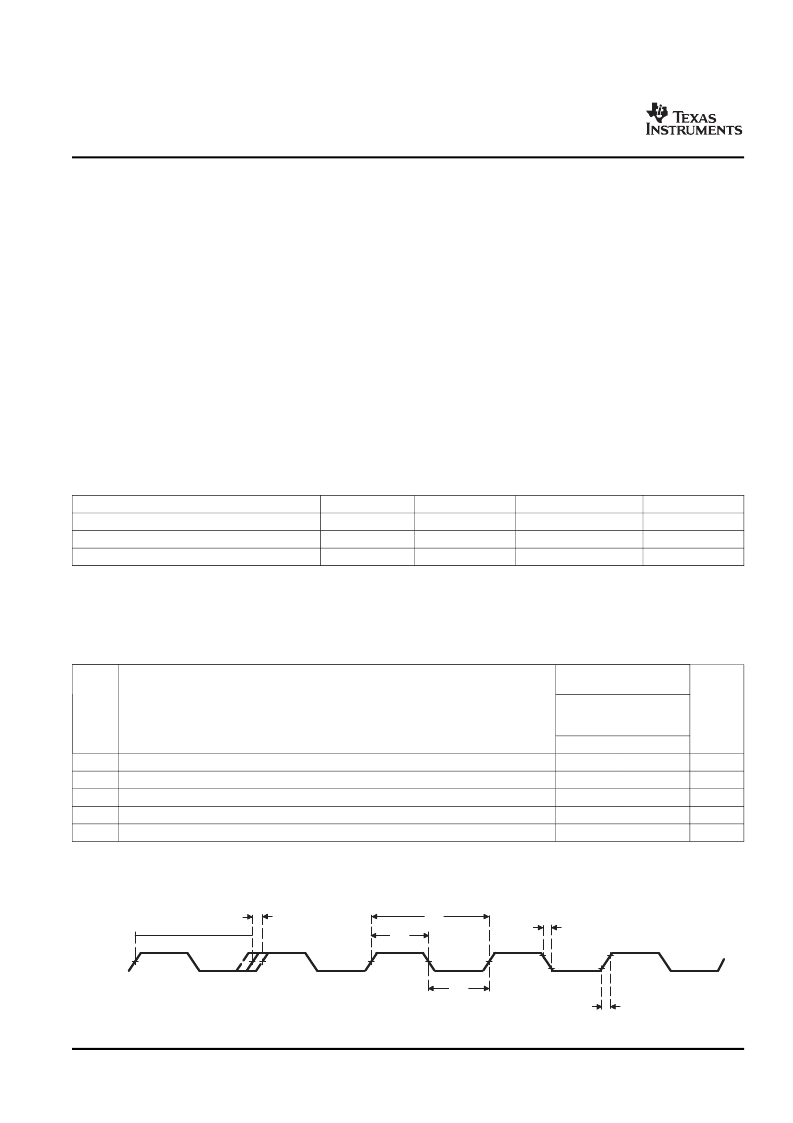
Table 6-8. Timing Requirements for CLKIN1
(1)(2)(3)
(see
Figure 6-6
)
-720
-900
PLL MODES
x1 (Bypass), x15, x20,
x25, x30, x32
MIN
15
0.4C
0.4C
NO.
UNIT
MAX
30.3
1
2
3
4
5
t
c(CLKIN1)
t
w(CLKIN1H)
t
w(CLKIN1L)
t
t(CLKIN1)
t
J(CLKIN1)
Cycle time, CLKIN1
Pulse duration, CLKIN1 high
Pulse duration, CLKIN1 low
Transition time, CLKIN1
Period jitter, (peak-to-peak), CLKIN1
ns
ns
ns
ns
ps
1.2
100
(1)
(2)
(3)
The reference points for the rise and fall transitions are measured at 3.3-V V
MAX and V
MIN.
C = CLKIN1 cycle time in ns. For example, when CLKIN1 frequency is 50 MHz, use C = 20 ns.
The PLL1 multiplier factors (x1 [BYPASS], x 15, x20, x25, x30, x32) further limit the MIN and MAX values for tc(CLKIN1). For more
detailed information on these limitations, see
Section 6.3.5
, DM647/DM648 Power and Clock Domains.
Figure 6-6. CLKIN1 Timing
Peripheral Information and Electrical Specifications
66
Submit Documentation Feedback
相關(guān)PDF資料 |
PDF描述 |
|---|---|
| TMS320DM647ZUT900 | Digital Media Processor |
| TMS320DM648ZUT720 | Digital Media Processor |
| TMS320DM648ZUT900 | Digital Media Processor |
| TMX320DM647ZUT720 | Digital Media Processor |
| TMX320DM647ZUT900 | Digital Media Processor |
相關(guān)代理商/技術(shù)參數(shù) |
參數(shù)描述 |
|---|---|
| TMS320DM647ZUT9 | 功能描述:數(shù)字信號(hào)處理器和控制器 - DSP, DSC Dig Media Proc RoHS:否 制造商:Microchip Technology 核心:dsPIC 數(shù)據(jù)總線寬度:16 bit 程序存儲(chǔ)器大小:16 KB 數(shù)據(jù) RAM 大小:2 KB 最大時(shí)鐘頻率:40 MHz 可編程輸入/輸出端數(shù)量:35 定時(shí)器數(shù)量:3 設(shè)備每秒兆指令數(shù):50 MIPs 工作電源電壓:3.3 V 最大工作溫度:+ 85 C 封裝 / 箱體:TQFP-44 安裝風(fēng)格:SMD/SMT |
| TMS320DM647ZUTA8 | 功能描述:數(shù)字信號(hào)處理器和控制器 - DSP, DSC Digital Media Proc RoHS:否 制造商:Microchip Technology 核心:dsPIC 數(shù)據(jù)總線寬度:16 bit 程序存儲(chǔ)器大小:16 KB 數(shù)據(jù) RAM 大小:2 KB 最大時(shí)鐘頻率:40 MHz 可編程輸入/輸出端數(shù)量:35 定時(shí)器數(shù)量:3 設(shè)備每秒兆指令數(shù):50 MIPs 工作電源電壓:3.3 V 最大工作溫度:+ 85 C 封裝 / 箱體:TQFP-44 安裝風(fēng)格:SMD/SMT |
| TMS320DM647ZUTD1 | 制造商:Texas Instruments 功能描述:- Trays |
| TMS320DM647ZUTD7 | 功能描述:數(shù)字信號(hào)處理器和控制器 - DSP, DSC Digital Media Proc RoHS:否 制造商:Microchip Technology 核心:dsPIC 數(shù)據(jù)總線寬度:16 bit 程序存儲(chǔ)器大小:16 KB 數(shù)據(jù) RAM 大小:2 KB 最大時(shí)鐘頻率:40 MHz 可編程輸入/輸出端數(shù)量:35 定時(shí)器數(shù)量:3 設(shè)備每秒兆指令數(shù):50 MIPs 工作電源電壓:3.3 V 最大工作溫度:+ 85 C 封裝 / 箱體:TQFP-44 安裝風(fēng)格:SMD/SMT |
| TMS320DM647ZUTD9 | 功能描述:數(shù)字信號(hào)處理器和控制器 - DSP, DSC Digital Media Proc RoHS:否 制造商:Microchip Technology 核心:dsPIC 數(shù)據(jù)總線寬度:16 bit 程序存儲(chǔ)器大小:16 KB 數(shù)據(jù) RAM 大小:2 KB 最大時(shí)鐘頻率:40 MHz 可編程輸入/輸出端數(shù)量:35 定時(shí)器數(shù)量:3 設(shè)備每秒兆指令數(shù):50 MIPs 工作電源電壓:3.3 V 最大工作溫度:+ 85 C 封裝 / 箱體:TQFP-44 安裝風(fēng)格:SMD/SMT |
發(fā)布緊急采購(gòu),3分鐘左右您將得到回復(fù)。