- 您現(xiàn)在的位置:買賣IC網(wǎng) > PDF目錄383959 > TMC22153AKHC (FAIRCHILD SEMICONDUCTOR CORP) JT 32C 32#20 SKT PLUG PDF資料下載
參數(shù)資料
| 型號(hào): | TMC22153AKHC |
| 廠商: | FAIRCHILD SEMICONDUCTOR CORP |
| 元件分類: | 顏色信號(hào)轉(zhuǎn)換 |
| 英文描述: | JT 32C 32#20 SKT PLUG |
| 中文描述: | COLOR SIGNAL DECODER, PQFP100 |
| 封裝: | MQFP-100 |
| 文件頁(yè)數(shù): | 9/84頁(yè) |
| 文件大小: | 417K |
| 代理商: | TMC22153AKHC |
第1頁(yè)第2頁(yè)第3頁(yè)第4頁(yè)第5頁(yè)第6頁(yè)第7頁(yè)第8頁(yè)當(dāng)前第9頁(yè)第10頁(yè)第11頁(yè)第12頁(yè)第13頁(yè)第14頁(yè)第15頁(yè)第16頁(yè)第17頁(yè)第18頁(yè)第19頁(yè)第20頁(yè)第21頁(yè)第22頁(yè)第23頁(yè)第24頁(yè)第25頁(yè)第26頁(yè)第27頁(yè)第28頁(yè)第29頁(yè)第30頁(yè)第31頁(yè)第32頁(yè)第33頁(yè)第34頁(yè)第35頁(yè)第36頁(yè)第37頁(yè)第38頁(yè)第39頁(yè)第40頁(yè)第41頁(yè)第42頁(yè)第43頁(yè)第44頁(yè)第45頁(yè)第46頁(yè)第47頁(yè)第48頁(yè)第49頁(yè)第50頁(yè)第51頁(yè)第52頁(yè)第53頁(yè)第54頁(yè)第55頁(yè)第56頁(yè)第57頁(yè)第58頁(yè)第59頁(yè)第60頁(yè)第61頁(yè)第62頁(yè)第63頁(yè)第64頁(yè)第65頁(yè)第66頁(yè)第67頁(yè)第68頁(yè)第69頁(yè)第70頁(yè)第71頁(yè)第72頁(yè)第73頁(yè)第74頁(yè)第75頁(yè)第76頁(yè)第77頁(yè)第78頁(yè)第79頁(yè)第80頁(yè)第81頁(yè)第82頁(yè)第83頁(yè)第84頁(yè)
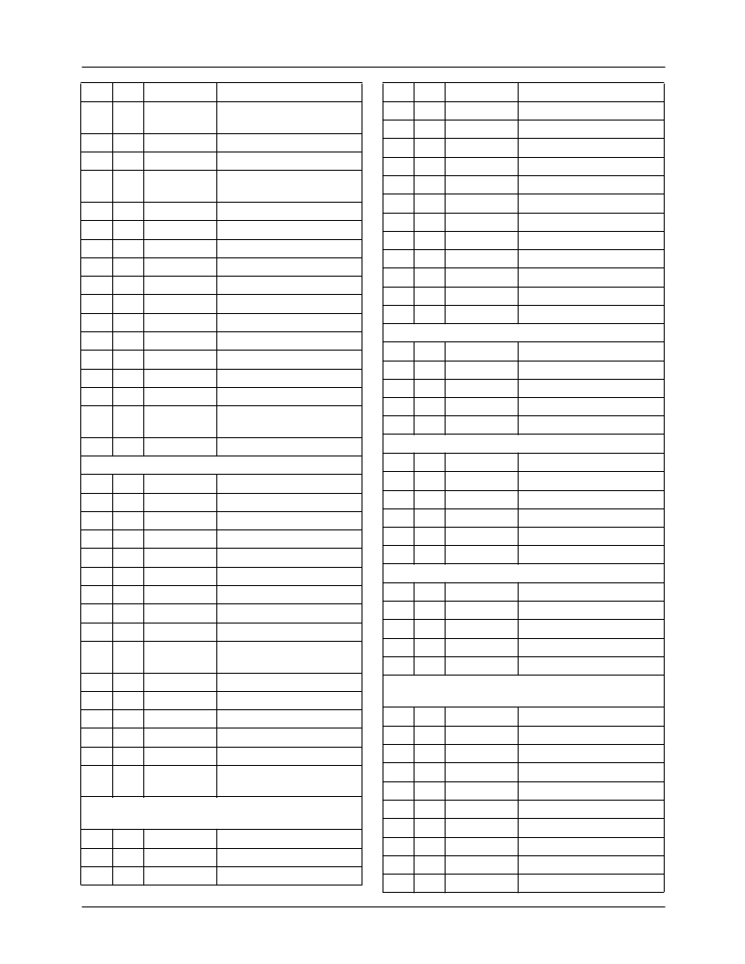
PRODUCT SPECIFICATION
TMC22x5yA
REV. 1.0.0 2/4/03
9
0D
7-6
CEST
Chroma error signal
transform
Chroma error signal gain
Luma error signal gain
Chroma error signal
bypass
XLUT filter enable
Adaption speed select
Luma weighting bypass
XLUT input select
XLUT special function
Y output select
C output select
reserved, set to zero
Adaption Threshold
D1 C
B
C
R
error signal
Comb filter input select
YC or Composite input
select
Sync processor select
Sync Pulse Generator
STS
7-0
Sync to sync 8 lsbs
STB
Sync to burst
BTV
Burst to video
AV
7-0
Active video line 8 lsbs
reserved, set to zero
AV
9-8
Active video line 2 msbs
reserved, set to zero
STS
10-8
Sync to sync 3 msbs
reserved, set to zero
VINDO
Number of lines in vertical
window
VDIV
Action inside VINDO
VDOV
Action outside VINDO
reserved, set to zero
NFDLY
new field detect delay
SPGIP
SPG input select
MSIP
Mixed sync separator input
select
Buffered register set 0
Active when BUFFER pin set LOW
7-0
SG0
7-0
Msync gain, 8 lsbs
7-0
YG0
7-0
Y gain, 8 lsbs
7-0
UG0
7-0
U gain, 8 lsbs
0D
0D
0D
5
4
3
CESG
YESG
CESTBY
0D
0D
0D
0E
0E
0E
0E
0F
0F
0F
0F
0F
2
1
0
XFEN
FAST
YWBY
XIP
XSF
YMUX
CMUX
7-6
5-4
3-2
1-0
7
6-5
4
3-2
1
CAT
DCES
IPCF
YCCOMP
0F
0
SYNC
10
11
12
13
14
14
14
14
15
15
7-0
7-0
7-0
7-0
7-6
5-4
3
2-0
7
6-2
15
15
16
16
16
16
1
0
7-6
5-4
3-2
1-0
17
18
19
Reg
Bit
Name
Function
1A
1B
1B
1B
1B
1C
1D
1D
1D
1E
1E
1F
7-0
7-6
5-3
2
1-0
7-0
7-3
2
1-0
7-1
0
7-0
VG0
7-0
YG0
9-8
UG0
10-8
V gain, 8 lsbs
Y gain, 2 msbs
U gain, 3 msbs
reserved, set to zero
V gain, 2 msbs
Y offset, 8 lsbs
reserved, set to zero
Y offset, msb
Msync gain, 2 msbs
7 lsbs of phase
V axis flip
8 msbs of phase
VG0
9-8
YOFF0
7-0
YOFF0
8
SG0
7-0
SYSPH0
6-0
VAXISO
SYSPH0
14-7
Normalized Subcarrier Frequency
7-4
FSC
3-0
3-0
7-0
FSC
11-4
7-0
FSC
19-12
7-0
FSC
27-20
Clamp Control
7
DRFSEL
6
PFLTBY
5-4
CLPSEL
1-0
3
VCLPEN
2-0
BAND
2-0
7-0
CPDLY
7-0
Output Format Control
7-6
5
LDVIO
4
OPCKS
3
DPCEN
2-0
DPC
Buffered register set 1
Active when BUFFER pin set HIGH
7-0
SG1
7-0
7-0
YG1
7-0
7-0
UG1
7-0
7-0
VG1
7-0
7-6
YG1
9-8
5-3
UG1
10-8
2
1-0
VG1
9-8
7-0
YOFF1
7-0
7-3
20
20
21
22
23
Bottom 4 bits of f
SC
reserved, set to zero
Lower 8 bits of f
SC
Middle 8 bits of f
SC
Top 8 bits of f
SC
24
24
24
24
24
25
Clamp pulse enable
Phase filter enable
Int. clamp selection
Clamp bypass
Clamp offset
Clamp pulse delay
26
26
26
26
26
reserved, set to zero
LDV clock select
Output clock select
DPC enable
Decoder product code
27
28
29
2A
2B
2B
2B
2B
2C
2D
Msync gain, 8 lsbs
Y gain, 8 lsbs
U gain, 8 lsbs
V gain, 8 lsbs
Y gain, 2 msbs
U gain, 3 msbs
reserved, set to zero
V gain, 2 msbs
Y offset, 8 lsbs
reserved, set to zero
Reg
Bit
Name
Function
相關(guān)PDF資料 |
PDF描述 |
|---|---|
| TMC3003R2C80 | Triple Video D/A Converter |
| TMC3003KRC30 | Triple Video D/A Converter |
| TMC3003KRC50 | Triple Video D/A Converter |
| TMC3003KRC80 | Triple Video D/A Converter |
| TMC3003 | Triple Video D/A Converter |
相關(guān)代理商/技術(shù)參數(shù) |
參數(shù)描述 |
|---|---|
| TMC22191 | 制造商:CADEKA 制造商全稱:CADEKA 功能描述:Digital Video Encoders/Layering Engine |
| TMC22191KHC | 功能描述:視頻 IC D/V Encoder Layering Engine RoHS:否 制造商:Fairchild Semiconductor 工作電源電壓:5 V 電源電流:80 mA 最大工作溫度:+ 85 C 封裝 / 箱體:TSSOP-28 封裝:Reel |
| TMC22191R0C | 功能描述:視頻 IC D/V Encoder Layering Engine RoHS:否 制造商:Fairchild Semiconductor 工作電源電壓:5 V 電源電流:80 mA 最大工作溫度:+ 85 C 封裝 / 箱體:TSSOP-28 封裝:Reel |
| TMC22191R0CT | 功能描述:視頻 IC D/V Encoder Layering Engine RoHS:否 制造商:Fairchild Semiconductor 工作電源電壓:5 V 電源電流:80 mA 最大工作溫度:+ 85 C 封裝 / 箱體:TSSOP-28 封裝:Reel |
| TMC222 | 制造商:Trinamic 功能描述:IC SM WITH I2C INTERFACE |
發(fā)布緊急采購(gòu),3分鐘左右您將得到回復(fù)。