- 您現(xiàn)在的位置:買賣IC網(wǎng) > PDF目錄383957 > TLV320AIC3106IGQER (Texas Instruments, Inc.) LOW-POWER STEREO AUDIO CODEC FOR PORTABLE AUDIO/TELEPHONY PDF資料下載
參數(shù)資料
| 型號: | TLV320AIC3106IGQER |
| 廠商: | Texas Instruments, Inc. |
| 元件分類: | Codec |
| 英文描述: | LOW-POWER STEREO AUDIO CODEC FOR PORTABLE AUDIO/TELEPHONY |
| 中文描述: | 低功耗立體聲音頻編解碼器的便攜式音頻/電話 |
| 文件頁數(shù): | 29/102頁 |
| 文件大小: | 1259K |
| 代理商: | TLV320AIC3106IGQER |
第1頁第2頁第3頁第4頁第5頁第6頁第7頁第8頁第9頁第10頁第11頁第12頁第13頁第14頁第15頁第16頁第17頁第18頁第19頁第20頁第21頁第22頁第23頁第24頁第25頁第26頁第27頁第28頁當(dāng)前第29頁第30頁第31頁第32頁第33頁第34頁第35頁第36頁第37頁第38頁第39頁第40頁第41頁第42頁第43頁第44頁第45頁第46頁第47頁第48頁第49頁第50頁第51頁第52頁第53頁第54頁第55頁第56頁第57頁第58頁第59頁第60頁第61頁第62頁第63頁第64頁第65頁第66頁第67頁第68頁第69頁第70頁第71頁第72頁第73頁第74頁第75頁第76頁第77頁第78頁第79頁第80頁第81頁第82頁第83頁第84頁第85頁第86頁第87頁第88頁第89頁第90頁第91頁第92頁第93頁第94頁第95頁第96頁第97頁第98頁第99頁第100頁第101頁第102頁
www.ti.com
STEREO AUDIO ADC
The TLV320AIC3106 includes a stereo audio ADC, which uses a delta-sigma modulator with 128-times
oversampling in single-rate mode, followed by a digital decimation filter. The ADC supports sampling rates from
8 kHz to 48 kHz in single-rate mode, and up to 96 kHz in dual-rate mode. Whenever the ADC or DAC is in
operation, the device requires an audio master clock be provided and appropriate audio clock generation be
setup within the part.
TLV320AIC3106
SLAS509B–DECEMBER 2006–REVISED JUNE 2007
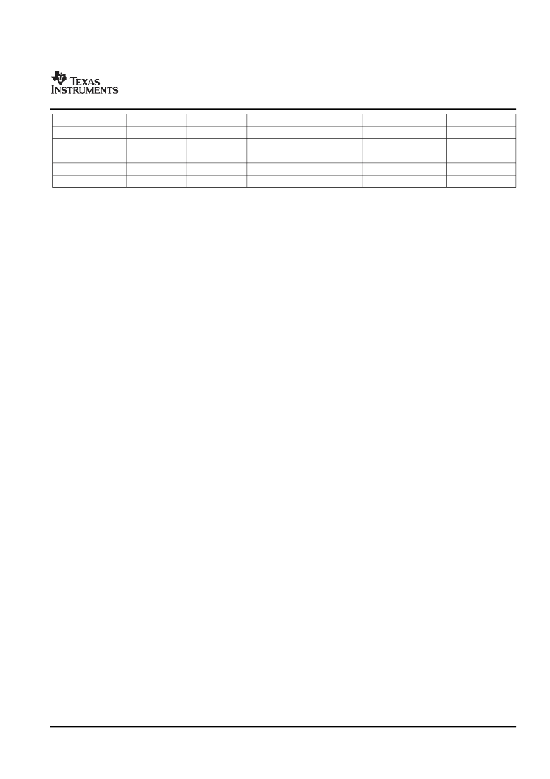
12.0
13.0
16.0
19.2
19.68
48.0
1
1
1
1
1
4
1
1
1
1
1
1
8
7
6
5
4
8
1920
5618
1440
1200
9951
1920
48000.00
47999.71
48000.00
48000.00
47999.79
48000.00
0.0000
–0.0006
0.0000
0.0000
–0.0004
0.0000
The AIC3106 can also output a separate clock on the GPIO1 pin. If the PLL is being used for the audio data
converter clock, the M and N settings can be used to provide a divided version of the PLL output. If the PLL is
not being used for the audio data converter clock, the PLL can still be enabled to provide a completely
independent clock output on GPIO1. The formula for the GPIO1 clock output when PLL is enabled and
CLKMUX_OUT is 0 is:
GPIO1 = (PLLCLK_IN
×
2
×
K
×
R) / (M
×
N
×
P)
When CLKMUX_OUT is 1, regardless of whether PLL is enabled or disabled, the input to the clock output
divider can be selected as MCLK, BCLK, or GPIO2. Is this case, the formula for the GPIO1 clock is:
GPIO1 = (CLKDIV_IN
×
2) / (M
×
N), where
M = 1, 2, 4, 8
N = 2, 3,
…
, 17
CLKDIV_IN can be BCLK, MCLK, or GPIO2, selected by page 0, register 102, bits D7-D6
In order to provide optimal system power dissipation, the stereo ADC can be powered one channel at a time, to
support the case where only mono record capability is required. In addition, both channels can be fully powered
or entirely powered down.
The integrated digital decimation filter removes high-frequency content and downsamples the audio data from an
initial sampling rate of 128 Fs to the final output sampling rate of Fs. The decimation filter provides a linear
phase output response with a group delay of 17/Fs. The –3 dB bandwidth of the decimation filter extends to 0.45
Fs and scales with the sample rate (Fs). The filter has minimum 75dB attenuation over the stopband from 0.55
Fs to 64 Fs. Independent digital highpass filters are also included with each ADC channel, with a corner
frequency that can be independently set to three different settings or can be disabled entirely.
Because of the oversampling nature of the audio ADC and the integrated digital decimation filtering,
requirements for analog anti-aliasing filtering are very relaxed. The TLV320AIC3106 integrates a second order
analog anti-aliasing filter with 20-dB attenuation at 1 MHz. This filter, combined with the digital decimation filter,
provides sufficient anti-aliasing filtering without requiring additional external components.
The ADC is preceded by a programmable gain amplifier (PGA), which allows analog gain control from 0 dB to
59.5 dB in steps of 0.5 dB. The PGA gain changes are implemented with an internal soft-stepping algorithm that
only changes the actual volume level by one 0.5-dB step every one or two ADC output samples, depending on
the register programming (see registers Page-0/Reg-19 and 22). This soft-stepping ensures that volume control
changes occur smoothly with no audible artifacts. On reset, the PGA gain defaults to a mute condition, and upon
power down, the PGA soft-steps the volume to mute before shutting down. A read-only flag is set whenever the
gain applied by PGA equals the desired value set by the register. The soft-stepping control can also be disabled
by programming a register bit. When soft stepping is enabled, the audio master clock must be applied to the part
after the ADC power down register is written to ensure the soft-stepping to mute has completed. When the ADC
powerdown flag is no longer set, the audio master clock can be shut down.
29
Submit Documentation Feedback
相關(guān)PDF資料 |
PDF描述 |
|---|---|
| TLV341_07 | LOW-VOLTAGE RAIL-TO-RAIL OUTPUT CMOS OPERATIONAL AMPLIFLERS WITH SHUTDOWN |
| TLV431ACDBV | LOW-VOLTAGE ADJUSTABLE PRECISION SHUNT REGULATORS |
| TLV431ID | LOW-VOLTAGE ADJUSTABLE PRECISION SHUNT REGULATORS |
| TLV431AIDBV | LOW-VOLTAGE ADJUSTABLE PRECISION SHUNT REGULATORS |
| TLV431ASNT1 | MS/STANDARD CYLINDRICAL MIL-C-5015 SERIES 3102A SOLID SHELL BOX MOUNT RECEPTACLES, STRAIGHT BODY STYLE, SOLDER TERMINATION, 14S SHELL SIZE, 14S-6 INSERT ARRANGEMENT, RECEPTACLE GENDER, 6 CONTACTS |
相關(guān)代理商/技術(shù)參數(shù) |
參數(shù)描述 |
|---|---|
| TLV320AIC3106IRGZR | 功能描述:接口—CODEC Lo-Pwr Stereo CODEC RoHS:否 制造商:Texas Instruments 類型: 分辨率: 轉(zhuǎn)換速率:48 kSPs 接口類型:I2C ADC 數(shù)量:2 DAC 數(shù)量:4 工作電源電壓:1.8 V, 2.1 V, 2.3 V to 5.5 V 最大工作溫度:+ 85 C 安裝風(fēng)格:SMD/SMT 封裝 / 箱體:DSBGA-81 封裝:Reel |
| TLV320AIC3106IRGZT | 功能描述:接口—CODEC Lo-Pwr Stereo CODEC RoHS:否 制造商:Texas Instruments 類型: 分辨率: 轉(zhuǎn)換速率:48 kSPs 接口類型:I2C ADC 數(shù)量:2 DAC 數(shù)量:4 工作電源電壓:1.8 V, 2.1 V, 2.3 V to 5.5 V 最大工作溫度:+ 85 C 安裝風(fēng)格:SMD/SMT 封裝 / 箱體:DSBGA-81 封裝:Reel |
| TLV320AIC3106IZQE | 功能描述:接口—CODEC Low-Power Stereo RoHS:否 制造商:Texas Instruments 類型: 分辨率: 轉(zhuǎn)換速率:48 kSPs 接口類型:I2C ADC 數(shù)量:2 DAC 數(shù)量:4 工作電源電壓:1.8 V, 2.1 V, 2.3 V to 5.5 V 最大工作溫度:+ 85 C 安裝風(fēng)格:SMD/SMT 封裝 / 箱體:DSBGA-81 封裝:Reel |
| TLV320AIC3106IZQER | 功能描述:接口—CODEC Low-Power Stereo RoHS:否 制造商:Texas Instruments 類型: 分辨率: 轉(zhuǎn)換速率:48 kSPs 接口類型:I2C ADC 數(shù)量:2 DAC 數(shù)量:4 工作電源電壓:1.8 V, 2.1 V, 2.3 V to 5.5 V 最大工作溫度:+ 85 C 安裝風(fēng)格:SMD/SMT 封裝 / 箱體:DSBGA-81 封裝:Reel |
| TLV320AIC3107 | 制造商:TI 制造商全稱:Texas Instruments 功能描述:LOW-POWER STEREO CODEC WITH INTEGRATED MONO CLASS-D SPEAKER AMPLIFIER |
發(fā)布緊急采購,3分鐘左右您將得到回復(fù)。