- 您現(xiàn)在的位置:買賣IC網(wǎng) > PDF目錄385814 > SAA7392HL (NXP SEMICONDUCTORS) Channel encoder/decoder CDR60 PDF資料下載
參數(shù)資料
| 型號: | SAA7392HL |
| 廠商: | NXP SEMICONDUCTORS |
| 元件分類: | 消費家電 |
| 英文描述: | Channel encoder/decoder CDR60 |
| 中文描述: | SPECIALTY CONSUMER CIRCUIT, PQFP80 |
| 封裝: | 12 X 12 MM, 1.40 MM HEIGHT, PLASTIC, MS-026, SOT-315-1, LQFP-80 |
| 文件頁數(shù): | 28/76頁 |
| 文件大小: | 246K |
| 代理商: | SAA7392HL |
第1頁第2頁第3頁第4頁第5頁第6頁第7頁第8頁第9頁第10頁第11頁第12頁第13頁第14頁第15頁第16頁第17頁第18頁第19頁第20頁第21頁第22頁第23頁第24頁第25頁第26頁第27頁當(dāng)前第28頁第29頁第30頁第31頁第32頁第33頁第34頁第35頁第36頁第37頁第38頁第39頁第40頁第41頁第42頁第43頁第44頁第45頁第46頁第47頁第48頁第49頁第50頁第51頁第52頁第53頁第54頁第55頁第56頁第57頁第58頁第59頁第60頁第61頁第62頁第63頁第64頁第65頁第66頁第67頁第68頁第69頁第70頁第71頁第72頁第73頁第74頁第75頁第76頁
2000 Mar 21
28
Philips Semiconductors
Preliminary specification
Channel encoder/decoder CDR60
SAA7392
Table 48
Motor Control Register 1 (address 0CH) - READ
7
6
5
4
3
2
1
0
ASCV.7
ASCV.6
ASCV.5
ASCV.4
ASCV.3
ASCV.2
ASCV.1
ASCV.0
7.6
Decoder function
7.6.1
D
EMODULATOR
The demodulator block includes sync extraction,
interpolation and protection circuits, and converts the
14-bit EFM data and subcode words into 8-bit symbols.
Two counters are used to detect frame synchronisation.
The coincidence counter detects the coincidence of
successive syncs (i.e. 2 syncs are within
588
±
1 EFM clock). The main counter partitions the EFM
signal into 16 or 17-bit bytes; and is reset when a sync
coincidence is found or the sync pulse is within
±
6 EFM
clock pulses. The sync coincidence signal generates the
‘lock’ signal which goes active HIGH when one sync
coincidence is found, and goes inactive when no sync
coincidence is found within 61 consecutive EFM frames.
The frame sync detection circuit extracts the frame sync
and will guard against mis-detection; up to 7 consecutive
corrupted syncs will not disturb the sync detection.
After data demodulation the sector sync is extracted; a
double lock counter is used. The main counter interpolates
the sector syncs, and a coincidence counter resets the
main counter.
7.6.2
E
RROR CORRECTOR
The error corrector can correct up to 2 errors on the
C1 level and up to 4 errors on the C2 level. The error
corrector also contains a flag processor. Flags are
assigned to symbols when the error corrector cannot
ascertain if the symbols are definitely good. C1 generates
output flags that are used by C2. The C2 output flags are
output via the FLAG signal along with the I
2
S, and can be
used by the interpolator for concealment of uncorrectable
errors for audio output.
Muting of data.
Data output via the serial interface
and/or the EBU can be set to zero using register
Output3.
Concealment of audio errors.
A simple 1 sample
linear interpolator can be selected via register Output3.
If selected the interpolator becomes active if a single
sample is flagged as erroneous; left and right channels
have independent interpolators.
7.6.2.1
CFLG pin
The error corrector outputs status information in serial
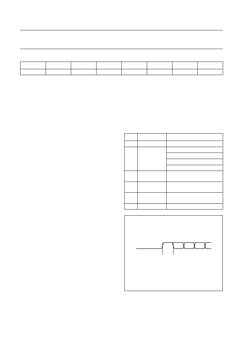
format on the CFLG pin. Each frame consists of 11 bits
(each 7 system clock periods long), beginning with a start
bit, then data bits then pause bit (see Fig.9). The repetition
rate of CFLG is not fixed; it depends on the disc speed and
output interface speed. There is always at least one pause
bit. The structure of the frame is shown in Table 49.
Table 49
Frame structure
BIT
VALUE
COMMENT
0
1 to 3 cormode<2:0>
logic 1
start bit
000 = C1 correction
011 = C2 correction
100 = corrector not active
all other codes not used
failure flag set because
correction impossible
failure flag set because
correction too risky
4
corfail
5
flagfail
6 to 9 rootcount<3:0> number of errors corrected,
after Euclidean algorithm
10
logic 0
pause bit
Fig.9 Format on CFLG pin.
MGR798
handbook, halfpage
bit 0
bit 1
start
bit
pause
data bits
bit 2
bit 3
相關(guān)PDF資料 |
PDF描述 |
|---|---|
| SAA7392 | Channel encoder/decoder CDR60(通道編碼器/譯碼器) |
| SAA7705H | Car radio Digital Signal Processor(DSP)(車載電臺數(shù)字信號處理器) |
| SAA7712H | Sound effects DSP(聲音效應(yīng)數(shù)字信號處理器) |
| SAA7712 | Sound effects DSP |
| SAA8110G | Digital Signal Processor (DSP) for cameras(應(yīng)用于照相中的數(shù)字信號處理器) |
相關(guān)代理商/技術(shù)參數(shù) |
參數(shù)描述 |
|---|---|
| SAA7500 | 制造商:PHILIPS 制造商全稱:NXP Semiconductors 功能描述:Digital satellite radio broadcasting tuner decoder SAT-2 |
| SAA7501WP | 制造商:未知廠家 制造商全稱:未知廠家 功能描述:ARD/ZDF NR.3R1 DIGITAL DECODER|LDCC|68PIN|PLASTIC |
| SAA-75J2.5-1 | 制造商:Amphenol Corporation 功能描述: |
| SAA7704H/204 | 制造商:NXP Semiconductors 功能描述:Electronic Component |
| SAA7705H | 制造商:PHILIPS 制造商全稱:NXP Semiconductors 功能描述:Car radio Digital Signal Processor DSP |
發(fā)布緊急采購,3分鐘左右您將得到回復(fù)。