- 您現(xiàn)在的位置:買賣IC網(wǎng) > PDF目錄385792 > S25FL001D0FNFI001 (SPANSION LLC) 2 Megabit, 1 Megabit CMOS 3.0 Volt Flash Memory with 25 MHz SPI Bus Interface PDF資料下載
參數(shù)資料
| 型號: | S25FL001D0FNFI001 |
| 廠商: | SPANSION LLC |
| 元件分類: | DRAM |
| 英文描述: | 2 Megabit, 1 Megabit CMOS 3.0 Volt Flash Memory with 25 MHz SPI Bus Interface |
| 中文描述: | 1M X 1 SPI BUS SERIAL EEPROM, PDSO8 |
| 封裝: | 6 X 5 MM, LEAD FREE, WSON-8 |
| 文件頁數(shù): | 24/38頁 |
| 文件大?。?/td> | 488K |
| 代理商: | S25FL001D0FNFI001 |
第1頁第2頁第3頁第4頁第5頁第6頁第7頁第8頁第9頁第10頁第11頁第12頁第13頁第14頁第15頁第16頁第17頁第18頁第19頁第20頁第21頁第22頁第23頁當前第24頁第25頁第26頁第27頁第28頁第29頁第30頁第31頁第32頁第33頁第34頁第35頁第36頁第37頁第38頁
24
S25FL Family (Serial Peripheral Interface)
30167A+1 June 9, 2004
P r e l i m i n a r y I n f o r m a t i o n
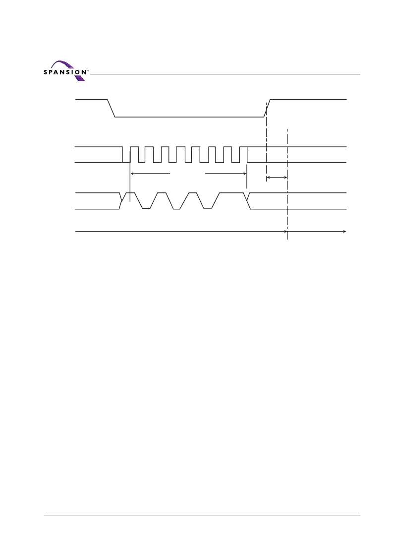
Figure 15. Release from Software Protect (RES) Instruction Sequence
Release from Software Protection and Read Electronic Signature (RES),
and Read ID (READ_ID)
Once the device has entered SP mode, all instructions are ignored except the RES
instruction. The RES instruction can also be used to read the 8-bit Electronic Sig-
nature of the device on the SO pin. The RES instruction always provides access
to the Electronic Signature of the device (except while an Erase, Program or
WRSR cycle is in progress), and can be applied even if SP mode has not been en-
tered. Any RES instruction executed while an Erase, Program or WRSR cycle is in
progress is not decoded, and has no effect on the cycle in progress.
The Read ID (READ_ID) instruction can be used to read, on Serial Data Output
(SO), the 8-bit Electronic Signature of the device.
Except while an Erase, Program or Write Status Register cycle is in progress, the
Read ID (READ_ID) instruction always provides access to the Electronic Signa-
ture of the device, and can be applied even if the Software Protect mode has not
been entered.
Any Read ID (READ_ID) instruction while an Erase, Program or Write Status Reg-
ister cycle is in progress, is not decoded, and has no effect on the cycle that is in
progress.
The device features an 8-bit Electronic Signature, whose value for the S25FL002D
is 11h, S25FL002D is 10h. This can be read using Read ID (READ_ID) instruction.
The device is first selected by driving Chip Select (CS#) Low. The instruction code
is followed by 3 dummy bytes, each bit being latched-in on Serial Data Input (SI)
during the rising edge of Serial Clock (SCK). Then, the 8-bit Electronic Signature,
stored in the memory, is shifted out on Serial Data Output (SO), each bit being
shifted out during the falling edge of Serial Clock (SCK).
The instruction sequence is shown in
Figure 16
.
The Read ID (READ_ID) instruction is terminated by driving Chip Select (CS#)
High after the Electronic Signature has been read at least once. Sending addi-
CS#
SCK
SI
0
1
2
3
4
5
6
7
Instruction
Software Protect Mode
t
RES
Standby Mode
相關(guān)PDF資料 |
PDF描述 |
|---|---|
| S25XXXH | SCR |
| S2516MH | SCR |
| S29GL032A30FFI012 | 64 Megabit, 32 Megabit, and 16 Megabit 3.0-Volt only Page Mode Flash Memory Featuring 200 nm MirrorBit Process Technology |
| S29GL032A100FAI013 | 64 Megabit, 32 Megabit, and 16 Megabit 3.0-Volt only Page Mode Flash Memory Featuring 200 nm MirrorBit Process Technology |
| S29GL032A100FAIR10 | 64 Megabit, 32 Megabit, and 16 Megabit 3.0-Volt only Page Mode Flash Memory Featuring 200 nm MirrorBit Process Technology |
相關(guān)代理商/技術(shù)參數(shù) |
參數(shù)描述 |
|---|---|
| S25FL001D0FNFI003 | 制造商:SPANSION 制造商全稱:SPANSION 功能描述:2 Megabit, 1 Megabit CMOS 3.0 Volt Flash Memory with 25 MHz SPI Bus Interface |
| S25FL001D0FNFI011 | 制造商:SPANSION 制造商全稱:SPANSION 功能描述:2 Megabit, 1 Megabit CMOS 3.0 Volt Flash Memory with 25 MHz SPI Bus Interface |
| S25FL001D0FNFI013 | 制造商:SPANSION 制造商全稱:SPANSION 功能描述:2 Megabit, 1 Megabit CMOS 3.0 Volt Flash Memory with 25 MHz SPI Bus Interface |
| S25FL002D | 制造商:SPANSION 制造商全稱:SPANSION 功能描述:2 Megabit, 1 Megabit CMOS 3.0 Volt Flash Memory with 25 MHz SPI Bus Interface |
| S25FL002D0FMAI001 | 制造商:SPANSION 制造商全稱:SPANSION 功能描述:2 Megabit, 1 Megabit CMOS 3.0 Volt Flash Memory with 25 MHz SPI Bus Interface |
發(fā)布緊急采購,3分鐘左右您將得到回復(fù)。