- 您現(xiàn)在的位置:買賣IC網(wǎng) > PDF目錄224993 > R1Q2A3609BBG-50RB 4M X 9 QDR SRAM, PBGA165 PDF資料下載
參數(shù)資料
| 型號: | R1Q2A3609BBG-50RB |
| 元件分類: | SRAM |
| 英文描述: | 4M X 9 QDR SRAM, PBGA165 |
| 封裝: | 15 X 17 MM, 1 MM PITCH, LEAD FREE, PLASTIC, LBGA-165 |
| 文件頁數(shù): | 4/26頁 |
| 文件大小: | 341K |
| 代理商: | R1Q2A3609BBG-50RB |
R1Q2A3636B/R1Q2A3618B/R1Q2A3609B
REJ03C0341-0003 Rev.0.03 Apr. 11, 2008
Page 12 of 24
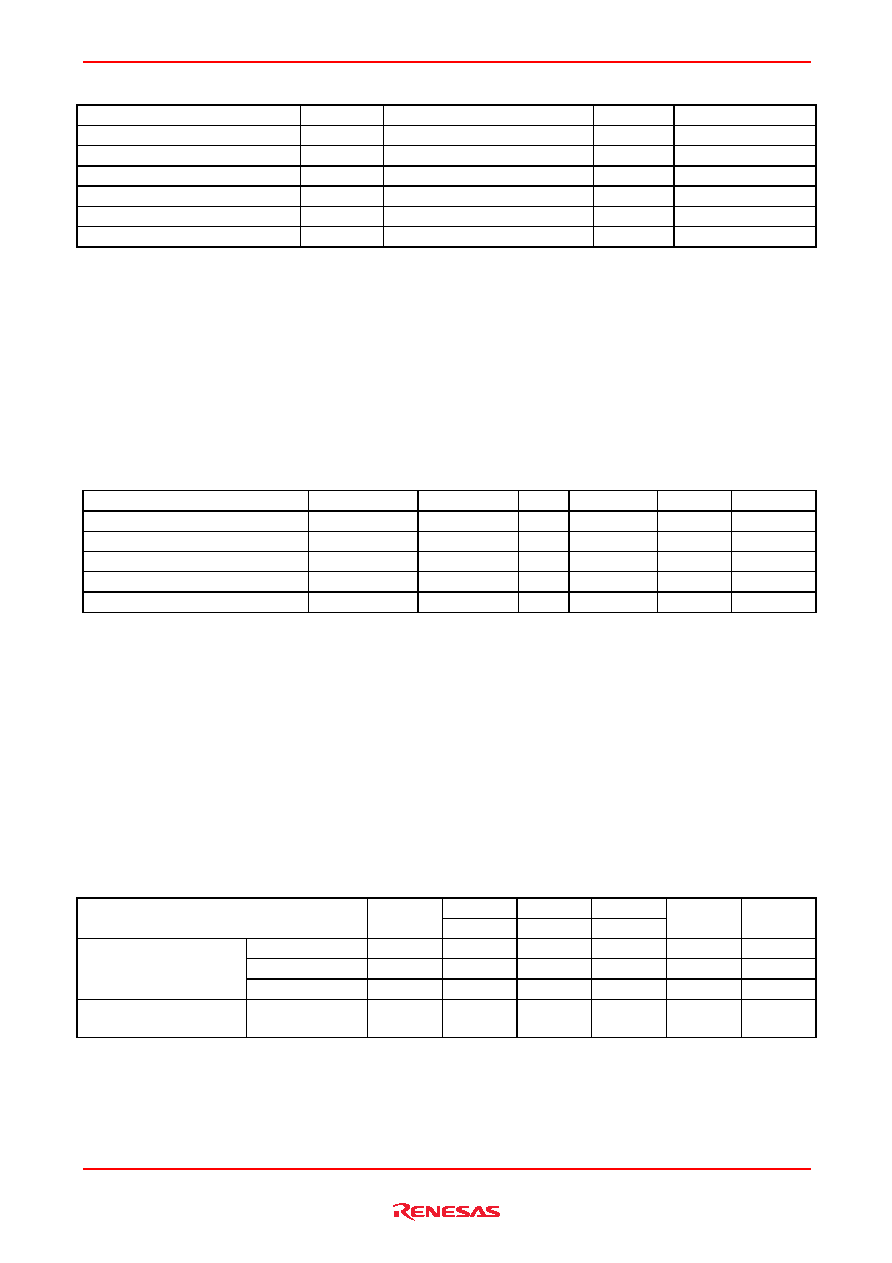
Absolute Maximum Ratings
Parameter
Symbol
Rating
Unit
Notes
Input voltage on any ball
VIN
0.5 to VDD + 0.5 (2.5 V max.)
V
1, 4
Input/output voltage
VI/O
0.5 to VDDQ + 0.5 (2.5 V max.)
V
1, 4
Core supply voltage
VDD
0.5 to 2.5
V
1, 4
Output supply voltage
VDDQ
0.5 to VDD
V
1, 4
Junction temperature
Tj
+125 (max)
°C
Storage temperature
TSTG
55 to +125
°C
Notes: 1. All voltage is referenced to VSS.
2. Permanent device damage may occur if Absolute Maximum Ratings are exceeded. Functional operation
should be restricted the Operation Conditions. Exposure to higher than recommended voltages for extended
periods of time could affect device reliability.
3. These CMOS memory circuits have been designed to meet the DC and AC specifications shown in the tables
after thermal equilibrium has been established.
4. The following supply voltage application sequence is recommended: VSS, VDD, VDDQ, VREF then VIN.
Remember, according to the Absolute Maximum Ratings table, VDDQ is not to exceed 2.5 V, whatever the
instantaneous value of VDDQ.
Recommended DC Operating Conditions
(Ta = 0 to +70°C)
Parameter
Symbol
Min
Typ
Max
Unit
Notes
Power supply voltage --core
VDD
1.7
1.8
1.9
V
Power supply voltage --I/O
VDDQ
1.4
1.5
VDD
V
Input reference voltage --I/O
VREF
0.68
0.75
0.95
V
1
Input high voltage
VIH (DC)
VREF
+ 0.1
VDDQ
+ 0.3
V
2, 3
Input low voltage
VIL (DC)
0.3
VREF
0.1
V
2, 3
Notes: 1. Peak to peak AC component superimposed on VREF may not exceed 5% of VREF.
2. Overshoot: VIH (AC)
≤ VDDQ + 0.5 V for t ≤ tKHKH/2
Undershoot: VIL (AC)
≥ 0.5 V for t ≤ tKHKH/2
Power-up: VIH
≤ VDDQ + 0.3 V and VDD ≤ 1.7 V and VDDQ ≤ 1.4 V for t ≤ 200 ms
During normal operation, VDDQ must not exceed VDD.
Control input signals may not have pulse widths less than tKHKL (min) or operate at cycle rates less than
tKHKH (min).
During normal operation, VIH(DC) must not exceed VDDQ and VIL(DC) must not be lower than VSS.
3. These are DC test criteria. The AC VIH / VIL levels are defined separately to measure timing parameters.
DC Characteristics
(Ta = 0 to +70
°C, VDD = 1.8V ± 0.1V)
40
50
60
Parameter
Symbol
Max
Unit
Notes
(×9)
IDD
600
550
500
mA
1, 2, 3
(×18)
IDD
650
600
550
mA
1, 2, 3
Operating supply current
(READ / WRITE)
(×36)
IDD
700
650
600
mA
1, 2, 3
Standby supply current
(NOP)
(×9 / ×18 / ×36)
ISB1
350
340
330
mA
2, 4, 5
相關(guān)PDF資料 |
PDF描述 |
|---|---|
| R1RP0408DGE-2PR | 512K X 8 STANDARD SRAM, 12 ns, PDSO36 |
| R251.375 | Axial Lead and Cartridge Fuses - Subminiature |
| R253.750 | Axial Lead and Cartridge Fuses - Subminiature |
| R284C0341008 | INTERCONNECTION DEVICE |
| R29683ASM/883B | 2K X 8 OTPROM, 85 ns, CDIP24 |
相關(guān)代理商/技術(shù)參數(shù) |
參數(shù)描述 |
|---|---|
| R1Q2A3609BBG-60R | 制造商:RENESAS 制造商全稱:Renesas Technology Corp 功能描述:36-Mbit QDR?II SRAM 2-word Burst |
| R1Q2A3609RBG-40RB0 | 制造商:RENESAS 制造商全稱:Renesas Technology Corp 功能描述:36-Mbit QDR?II SRAM 2-word Burst |
| R1Q2A3609RBG-40RS0 | 制造商:RENESAS 制造商全稱:Renesas Technology Corp 功能描述:36-Mbit QDR?II SRAM 2-word Burst |
| R1Q2A3609RBG-40RT0 | 制造商:RENESAS 制造商全稱:Renesas Technology Corp 功能描述:36-Mbit QDR?II SRAM 2-word Burst |
| R1Q2A3609RBG-50RB0 | 制造商:RENESAS 制造商全稱:Renesas Technology Corp 功能描述:36-Mbit QDR?II SRAM 2-word Burst |
發(fā)布緊急采購,3分鐘左右您將得到回復。