- 您現在的位置:買賣IC網 > PDF目錄296800 > PEF22508E (INFINEON TECHNOLOGIES AG) DATACOM, PCM TRANSCEIVER, PBGA256 PDF資料下載
參數資料
| 型號: | PEF22508E |
| 廠商: | INFINEON TECHNOLOGIES AG |
| 元件分類: | 數字傳輸電路 |
| 英文描述: | DATACOM, PCM TRANSCEIVER, PBGA256 |
| 封裝: | 17 X 17 MM, 1 MM PITCH, PLASTIC, LBGA-256 |
| 文件頁數: | 134/193頁 |
| 文件大?。?/td> | 10683K |
| 代理商: | PEF22508E |
第1頁第2頁第3頁第4頁第5頁第6頁第7頁第8頁第9頁第10頁第11頁第12頁第13頁第14頁第15頁第16頁第17頁第18頁第19頁第20頁第21頁第22頁第23頁第24頁第25頁第26頁第27頁第28頁第29頁第30頁第31頁第32頁第33頁第34頁第35頁第36頁第37頁第38頁第39頁第40頁第41頁第42頁第43頁第44頁第45頁第46頁第47頁第48頁第49頁第50頁第51頁第52頁第53頁第54頁第55頁第56頁第57頁第58頁第59頁第60頁第61頁第62頁第63頁第64頁第65頁第66頁第67頁第68頁第69頁第70頁第71頁第72頁第73頁第74頁第75頁第76頁第77頁第78頁第79頁第80頁第81頁第82頁第83頁第84頁第85頁第86頁第87頁第88頁第89頁第90頁第91頁第92頁第93頁第94頁第95頁第96頁第97頁第98頁第99頁第100頁第101頁第102頁第103頁第104頁第105頁第106頁第107頁第108頁第109頁第110頁第111頁第112頁第113頁第114頁第115頁第116頁第117頁第118頁第119頁第120頁第121頁第122頁第123頁第124頁第125頁第126頁第127頁第128頁第129頁第130頁第131頁第132頁第133頁當前第134頁第135頁第136頁第137頁第138頁第139頁第140頁第141頁第142頁第143頁第144頁第145頁第146頁第147頁第148頁第149頁第150頁第151頁第152頁第153頁第154頁第155頁第156頁第157頁第158頁第159頁第160頁第161頁第162頁第163頁第164頁第165頁第166頁第167頁第168頁第169頁第170頁第171頁第172頁第173頁第174頁第175頁第176頁第177頁第178頁第179頁第180頁第181頁第182頁第183頁第184頁第185頁第186頁第187頁第188頁第189頁第190頁第191頁第192頁第193頁
Data Sheet
45
Rev. 1.0, 2005-06-02
OctalLIU
TM
PEF 22508 E
Functional Description
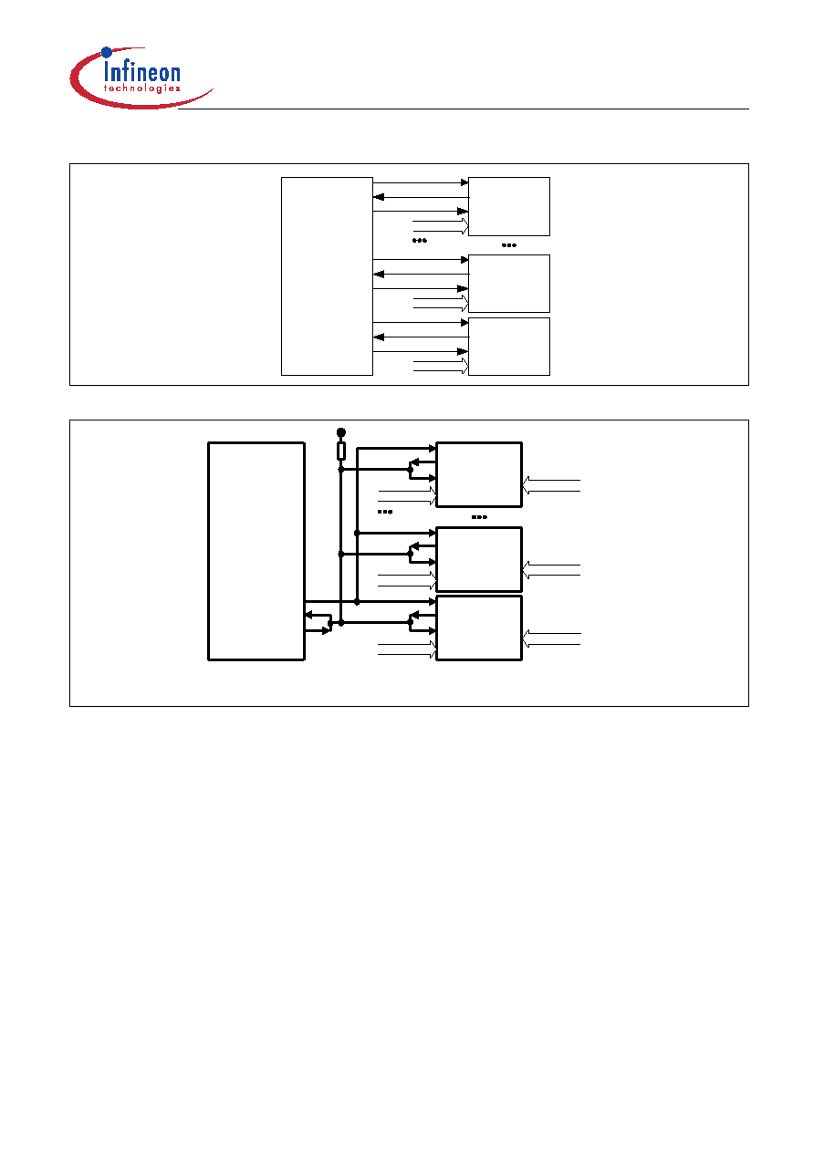
Figure 6
SCI Interface Application with Point To Point Connections
Figure 7
SCI Interface Application with Multipoint To Multipoint Connection
The following configurations of the SCI interface of the OctalLIU
TM can be set by the micro controller by a write
command into the SCI configuration register (control bits 10
Half duplex/full duplex (reset value: Half duplex), bit DUP.
OpenDrain/push-pull (configuration of output pin to openDrain/push-pull is in general independent of the
duplex mode and must be set appropriately in application) (reset value: open Drain), bit PP.
CRC for transmit and receive on/off (reset value: off), bit CRC_EN.
Automatic acknowledgement of CMD messages on/off (reset value: off), bit ACK_EN.
Clock edge rising/falling (reset value: falling), bit CLK_POL.
Clock gating (reset value: off), bit CLK_GAT.
The following SCI configurations are fixed and cannot be set by the micro controller:
Interrupt feature is disabled, bit INT_EN = 0
B.
Arbitration always made with LAPD (only SCI applications like in Figure 6 and Figure 7 are possible), bit ARB
= 0
B.
The maximum possible SCI clock frequency is 6 MHz for point to point applications (full duplex) and about 2 MHz
for multipoint to multipoint applications, dependent on the electrical capacity of the bus lines of the PCB.
Figure 8 shows the message structure of the OctalLIU
TM. The SCI interface uses HDLC frames for
communication. The HDLC flags mark beginning and end of all messages.
Microprocessor
or
Interworking
Device
IM(1:0)
TxData
RxData
Clk
TxData
RxData
Clk
TxData
RxData
Clk
OctalLIU
SCI_TXD
SCI_RXD
PP
OctalLIU
OctalLIU-Interfaces_2
Micro-processor
or
Interworking
Device
IM(1:0)
Clk
OctalLIU_SCI_halfduplex
A(5:0)
SCI_RXD
oD
OctalLIU
SCI_TXD
Data
OctalLIU
相關PDF資料 |
PDF描述 |
|---|---|
| PEF22554E | DATACOM, FRAMER, PBGA160 |
| PEF22554HT | DATACOM, FRAMER, PQFP144 |
| PES12-42S-N0024 | |
| PESD3V3V4UK,132 | 25 W, UNIDIRECTIONAL, 4 ELEMENT, SILICON, TVS DIODE |
| PF38F3050L0YUQ3A | SPECIALTY MEMORY CIRCUIT, PBGA88 |
相關代理商/技術參數 |
參數描述 |
|---|---|
| PEF22508EV1.1-G | 功能描述:網絡控制器與處理器 IC T/E RoHS:否 制造商:Micrel 產品:Controller Area Network (CAN) 收發(fā)器數量: 數據速率: 電源電流(最大值):595 mA 最大工作溫度:+ 85 C 安裝風格:SMD/SMT 封裝 / 箱體:PBGA-400 封裝:Tray |
| PEF22508EV11G | 制造商:Rochester Electronics LLC 功能描述: 制造商:Infineon Technologies AG 功能描述: |
| PEF22508EV11GXP | 制造商:Lantiq 功能描述:LINE INTERFACE UNITS |
| PEF22508EV11GXT | 制造商:Lantiq 功能描述:LINE INTERFACE UNITS |
| PEF22509EV1.1 | 制造商:Infineon Technologies AG 功能描述:SP000205605_T/E ASIC_TY_PB |
發(fā)布緊急采購,3分鐘左右您將得到回復。