- 您現(xiàn)在的位置:買賣IC網(wǎng) > PDF目錄384755 > MT48LC2M32B2 (Micron Technology, Inc.) SYNCHRONOUS DRAM PDF資料下載
參數(shù)資料
| 型號: | MT48LC2M32B2 |
| 廠商: | Micron Technology, Inc. |
| 英文描述: | SYNCHRONOUS DRAM |
| 中文描述: | 同步DRAM |
| 文件頁數(shù): | 37/53頁 |
| 文件大小: | 1818K |
| 代理商: | MT48LC2M32B2 |
第1頁第2頁第3頁第4頁第5頁第6頁第7頁第8頁第9頁第10頁第11頁第12頁第13頁第14頁第15頁第16頁第17頁第18頁第19頁第20頁第21頁第22頁第23頁第24頁第25頁第26頁第27頁第28頁第29頁第30頁第31頁第32頁第33頁第34頁第35頁第36頁當(dāng)前第37頁第38頁第39頁第40頁第41頁第42頁第43頁第44頁第45頁第46頁第47頁第48頁第49頁第50頁第51頁第52頁第53頁
37
64Mb: x32 SDRAM
64MSDRAMx32_5.p65 – Rev. B; Pub. 6/02
Micron Technology, Inc., reserves the right to change products or specifications without notice.
2002, Micron Technology, Inc.
64Mb: x32
SDRAM
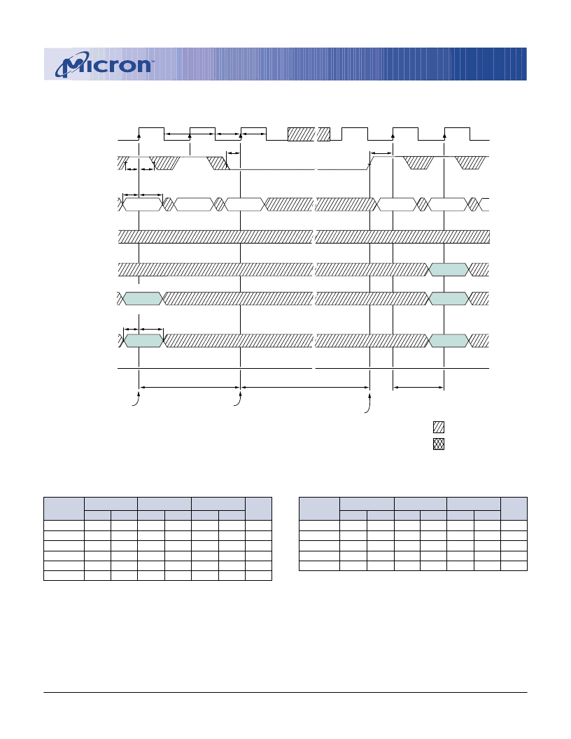
NOTE:
1. Violating refresh requirements during power-down may result in a loss of data.
POWER-DOWN MODE
1
*CAS latency indicated in parentheses.
-5
-6
-7
SYMBOL*
t
CK (1)
t
CKH
t
CKS
t
CMH
t
CMS
MIN
MAX
MIN
20
1
1.5
1
1.5
MAX
MIN
20
1
2
1
2
MAX
UNITS
ns
ns
ns
ns
ns
1
1.5
1
1.5
TIMING PARAMETERS
-5
-6
-7
SYMBOL*
t
AH
t
AS
t
CH
t
CL
t
CK (3)
t
CK (2)
MIN
1
1.5
2
2
5
MAX
MIN
1
1.5
2.5
2.5
6
10
MAX
MIN
1
2
2.75
2.75
7
10
MAX
UNITS
ns
ns
ns
ns
ns
ns
tCH
tCL
tCK
Two clock cycles
CKE
CLK
DQ
All banks idle, enter
power-down mode
Precharge all
active banks
Input buffers gated off while in
power-down mode
Exit power-down mode
(
)
(
)
(
)
(
)
tCKS
tCKS
COMMAND
tCMH
tCMS
PRECHARGE
NOP
NOP
ACTIVE
NOP
(
)
(
)
(
)
(
)
All banks idle
BA0, BA1
BANK
BANK(S)
(
)
(
)
(
)
(
)
High-Z
tAH
tAS
tCKH
tCKS
DQM 0-3
(
)
(
)
(
)
(
)
(
)
(
)
(
)
(
)
A0-A9
ROW
(
)
(
)
(
)
(
)
ALL BANKS
SINGLE BANK
A10
ROW
(
)
(
)
(
)
(
)
T0
T1
T2
Tn + 1
Tn + 2
DON’T CARE
UNDEFINED
相關(guān)PDF資料 |
PDF描述 |
|---|---|
| MT48LC32M8A2 | SYNCHRONOUS DRAM |
| MT48LC16M16A2 | SYNCHRONOUS DRAM |
| MT48LC64M4A2 | SYNCHRONOUS DRAM |
| MT48LC4M32B2 | SYNCHRONOUS DRAM |
| MT48LC4M32LFFC | SYNCHRONOUS DRAM |
相關(guān)代理商/技術(shù)參數(shù) |
參數(shù)描述 |
|---|---|
| MT48LC2M32B2-6G | 制造商:Micron Technology Inc 功能描述: |
發(fā)布緊急采購,3分鐘左右您將得到回復(fù)。