- 您現(xiàn)在的位置:買賣IC網(wǎng) > PDF目錄296559 > MIC2591B-5YTQ (MICREL INC) 1-CHANNEL POWER SUPPLY SUPPORT CKT, PQFP48 PDF資料下載
參數(shù)資料
| 型號: | MIC2591B-5YTQ |
| 廠商: | MICREL INC |
| 元件分類: | 電源管理 |
| 英文描述: | 1-CHANNEL POWER SUPPLY SUPPORT CKT, PQFP48 |
| 封裝: | LEAD FREE, TQFP-48 |
| 文件頁數(shù): | 30/34頁 |
| 文件大?。?/td> | 1920K |
| 代理商: | MIC2591B-5YTQ |
第1頁第2頁第3頁第4頁第5頁第6頁第7頁第8頁第9頁第10頁第11頁第12頁第13頁第14頁第15頁第16頁第17頁第18頁第19頁第20頁第21頁第22頁第23頁第24頁第25頁第26頁第27頁第28頁第29頁當前第30頁第31頁第32頁第33頁第34頁
March 2005
5
M9999-033105
MIC2591B
Micrel
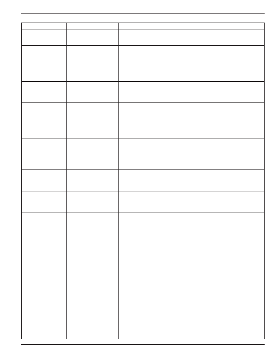
Pin Description (continued)
Pin Number
Pin Name
Pin Function
33
IREF
A resistor connected between this pin and GND sets the ADC current
measurement gain for the VAUX[A/B] outputs. This resistor must be
23.2kΩ±1%.
11
VSTBYA
3.3V Standby Input Voltage: Required to support PCI Express VAUX
26
VSTBYB
output(s). These inputs are the primary supply for the MIC2591B and must
be applied at all times for the controller to function properly.
Additionally, the SMBus logic and internal registers run off of VSTBY[A/B]
to ensure that the chip is accessible during standby modes. A UVLO circuit
prevents turn-on of this supply until VSTBY[A/B] rises above its UVLO
threshold. Both pins must be connected together at the MIC2591B controller.
15
VAUXA
3.3VAUX Outputs to PCI Express Card Slots: These outputs connect
22
VAUXB
the 3.3AUX pin of the PCI Express connectors to VSTBY[A/B] via internal
400mΩ MOSFETs. These outputs are current limited and protected against
short-circuit faults.
44
ONA
Enable Inputs: Rising-edge triggered. Used to enable or disable the MAINA
43
ONB
and MAINB (+3.3V and +12V) outputs. The outputs can be switched on by
these controls only after the VSTBY input supply is valid and stabe (i.e., t
STBY
POR
elapses - See the Electrical Characteristics Table). Taking ON[A/B] low after
a fault resets the +12V and/or +3.3V fault latches for the affected slot. Tie
these pins to GND if using SMI power control. Also, see pin description for
/FAULTA and /FAULTB.
45
AUXENA
Enable Inputs: Rising-edge triggered. Used to enable or disable the
42
AUXENB
VAUX[A/B] outputs. The outputs can be switched on by these controls only
after the VSTBY input supply is valid and stabe (i.e., t
STBY
POR elapses - See the
Electrical Characteristics Table).Taking AUXEN[A/B] low after a fault resets
the respective slot’s Aux Output Fault Latch. Tie these pins to GND if using
SMI power control. Also, see pin description for /FAULTA and /FAULTB.
2
CFILTERA
Overcurrent Timers: Capacitors connected between these
35
CFILTERB
pins and GND set the duration of tFLT for each slot. The overcurrent lter
delay (tFLT) is the amount of time for which a slot remains in current limit
before its circuit breaker is tripped.
6
/PWRGDA
Power-is-Good Outputs: Open-drain, active-low. Asserted when a slot has
31
/PWRGDB
been commanded to turn on and has successfully begun delivering power
to its respective +12V, +3.3V, and VAUX outputs. Each pin requires an
external pull-up resistor to VSTBY.
STBY
1
/FAULTA
Fault Outputs: Open-drain, active-low. Asserted whenever the
36
/FAULTB
circuit breaker trips due to a fault condition (overcurrent, input undervoltage,
overtemperature). Each pin requires an external pull-up resistor to VSTBY.
STBY
Bringing the slot’s ON[A/B] pin low resets /FAULT[A/B] if /FAULT[A/B]
was asserted in response to a fault condition on one of the slot’s MAIN out-
puts (+12V or +3.3V).
/FAULT[A/B] is reset by bringing the slot’s AUXEN[A/B] pin low if
/FAULT[A/B] was asserted in response to a fault condition on the slot’s VAUX
output. If a fault condition occurred on both the MAIN and VAUX outputs of
the same slot, then both ON[A/B] and AUXEN[A/B] must be brought low to
deassert the /FAULT[A/B] output.
9
/FORCE_ONA
Enable Inputs: Active-low, level-sensitive. Asserting a /FORCE_ON[A/B]
28
/FORCE_ONB
input will turn on all three of the respective slot’s outputs (+12V, +3.3V, and
VAUX), while specically defeating all protections on those supplies. This
explcitly includes all overcurrent and short circuit protections, and on-chip
thermal protection for the VAUX[A/B] supplies. Additionally included are the
UVLO protections for the +3.3V and +12V main supplies. The
/FORCE_ON[A/B] pins do not disable UVLO protection for the VAUX[A/B]
supplies. These input pins are intended for diagnostic purposes only.
Asserting /FORCE_ON[A/B] will cause the respective slot’s /PWRGD[A/B]
and /FAULT[A/B] pins to enter their open-drain state. Note that the SMBus
register set will continue to reect the actual state of each slot’s supplies.
There is a pair of register bits, accessible via the SMBus, which can be set
to disable (unconditionally deassert) either or both of the /FORCE_ON[A/B]
pins -- See CNTRL[A/B] Register Bit D[2].
Pin Number
Pin Name
Pin Function
33
IREF
A resistor connected between this pin and GND sets the ADC current
measurement gain for the VAUX[A/B] outputs. This resistor must be
23.2kΩ±1%.
be applied at all times for the controller to function properly.
Additionally, the SMBus logic and internal registers run off of VSTBY[A/B]
to ensure that the chip is accessible during standby modes. A UVLO circuit
22
VAUXB
the 3.3AUX pin of the PCI Express connectors to VSTBY[A/B] via internal
43
ONB
and MAINB (+3.3V and +12V) outputs. The outputs can be switched on by
45
AUXENA
Enable Inputs: Rising-edge triggered. Used to enable or disable the
42
AUXENB
VAUX[A/B] outputs.
2
CFILTERA
Overcurrent Timers: Capacitors connected between these
35
CFILTERB
pins and GND set the duration of t
delay (t
before its circuit breaker is tripped.
6
/PWRGDA
Power-is-Good Outputs: Open-drain, active-low. Asserted when a slot has
31
/PWRGDB
been commanded to turn on and has successfully begun delivering power
1
/FAULTA
Fault Outputs: Open-drain, active-low. Asserted whenever the
36
/FAULTB
circuit breaker trips due to a fault condition (overcurrent, input undervoltage,
9
/FORCE_ONA
Enable Inputs: Active-low, level-sensitive. Asserting a /FORCE_ON[A/B]
28
/FORCE_ONB
input will turn on all three of the respective slot’s outputs (+12V, +3.3V, and
There is a pair of register bits, accessible via the SMBus, which can be set
Pin Number
Pin Name
Pin Function
33
IREF
A resistor connected between this pin and GND sets the ADC current
measurement gain for the VAUX[A/B] outputs. This resistor must be
23.2kΩ±1%.
11
VSTBYA
3.3V Standby Input Voltage: Required to support PCI Express VAUX
be applied at all times for the controller to function properly.
Additionally, the SMBus logic and internal registers run off of VSTBY[A/B]
to ensure that the chip is accessible during standby modes. A UVLO circuit
15
VAUXA
3.3VAUX Outputs to PCI Express Card Slots: These outputs connect
22
VAUXB
the 3.3AUX pin of the PCI Express connectors to VSTBY[A/B] via internal
44
ONA
Enable Inputs: Rising-edge triggered. Used to enable or disable the MAINA
43
ONB
and MAINB (+3.3V and +12V) outputs. The outputs can be switched on by
45
AUXENA
Enable Inputs: Rising-edge triggered. Used to enable or disable the
42
AUXENB
VAUX[A/B] outputs.
2
CFILTERA
Overcurrent Timers: Capacitors connected between these
35
CFILTERB
pins and GND set the duration of t
delay (t
before its circuit breaker is tripped.
6
/PWRGDA
Power-is-Good Outputs: Open-drain, active-low. Asserted when a slot has
31
/PWRGDB
been commanded to turn on and has successfully begun delivering power
1
/FAULTA
Fault Outputs: Open-drain, active-low. Asserted whenever the
36
/FAULTB
circuit breaker trips due to a fault condition (overcurrent, input undervoltage,
9
/FORCE_ONA
Enable Inputs: Active-low, level-sensitive. Asserting a /FORCE_ON[A/B]
28
/FORCE_ONB
input will turn on all three of the respective slot’s outputs (+12V, +3.3V, and
There is a pair of register bits, accessible via the SMBus, which can be set
Pin Number
Pin Name
Pin Function
33
IREF
A resistor connected between this pin and GND sets the ADC current
measurement gain for the VAUX[A/B] outputs. This resistor must be
23.2kΩ±1%.
11
VSTBYA
3.3V Standby Input Voltage: Required to support PCI Express VAUX
output(s). These inputs are the primary supply for the MIC2591B and must
be applied at all times for the controller to function properly.
Additionally, the SMBus logic and internal registers run off of VSTBY[A/B]
to ensure that the chip is accessible during standby modes. A UVLO circuit
15
VAUXA
3.3VAUX Outputs to PCI Express Card Slots: These outputs connect
22
VAUXB
the 3.3AUX pin of the PCI Express connectors to VSTBY[A/B] via internal
44
ONA
Enable Inputs: Rising-edge triggered. Used to enable or disable the MAINA
43
ONB
and MAINB (+3.3V and +12V) outputs. The outputs can be switched on by
45
AUXENA
Enable Inputs: Rising-edge triggered. Used to enable or disable the
42
AUXENB
VAUX[A/B] outputs.
2
CFILTERA
Overcurrent Timers: Capacitors connected between these
35
CFILTERB
pins and GND set the duration of t
delay (t
before its circuit breaker is tripped.
6
/PWRGDA
Power-is-Good Outputs: Open-drain, active-low. Asserted when a slot has
31
/PWRGDB
been commanded to turn on and has successfully begun delivering power
1
/FAULTA
Fault Outputs: Open-drain, active-low. Asserted whenever the
36
/FAULTB
circuit breaker trips due to a fault condition (overcurrent, input undervoltage,
9
/FORCE_ONA
Enable Inputs: Active-low, level-sensitive. Asserting a /FORCE_ON[A/B]
28
/FORCE_ONB
input will turn on all three of the respective slot’s outputs (+12V, +3.3V, and
There is a pair of register bits, accessible via the SMBus, which can be set
相關(guān)PDF資料 |
PDF描述 |
|---|---|
| MIC30711-5100W-LF3 | 32 CONTACT(S), FEMALE, RIGHT ANGLE TELECOM AND DATACOM CONNECTOR, SOLDER |
| MIC3730-1.8BR | 1.8 V FIXED POSITIVE LDO REGULATOR, 0.5 V DROPOUT, PSSO5 |
| MIC5225-1.5YM5TR | 1.5 V FIXED POSITIVE LDO REGULATOR, 0.45 V DROPOUT, PDSO5 |
| MIC5225-2.5YM5TR | 2.5 V FIXED POSITIVE LDO REGULATOR, 0.45 V DROPOUT, PDSO5 |
| MIC5225-3.3YM5TR | 3.3 V FIXED POSITIVE LDO REGULATOR, 0.45 V DROPOUT, PDSO5 |
相關(guān)代理商/技術(shù)參數(shù) |
參數(shù)描述 |
|---|---|
| MIC2592B-2BTQ | 功能描述:IC CTRLR HOTPLUG PCI DUAL 48TQFP RoHS:否 類別:集成電路 (IC) >> PMIC - 熱交換 系列:- 產(chǎn)品培訓(xùn)模塊:Obsolescence Mitigation Program 標準包裝:100 系列:- 類型:熱插拔開關(guān) 應(yīng)用:通用 內(nèi)部開關(guān):是 電流限制:可調(diào) 電源電壓:9 V ~ 13.2 V 工作溫度:-40°C ~ 150°C 安裝類型:表面貼裝 封裝/外殼:10-WFDFN 裸露焊盤 供應(yīng)商設(shè)備封裝:10-TDFN-EP(3x3) 包裝:管件 |
| MIC2592B-2BTQ TR | 功能描述:IC PCI HOT PLUG CTLR DUAL 48TQFP RoHS:否 類別:集成電路 (IC) >> PMIC - 熱交換 系列:- 產(chǎn)品培訓(xùn)模塊:Obsolescence Mitigation Program 標準包裝:100 系列:- 類型:熱插拔開關(guān) 應(yīng)用:通用 內(nèi)部開關(guān):是 電流限制:可調(diào) 電源電壓:9 V ~ 13.2 V 工作溫度:-40°C ~ 150°C 安裝類型:表面貼裝 封裝/外殼:10-WFDFN 裸露焊盤 供應(yīng)商設(shè)備封裝:10-TDFN-EP(3x3) 包裝:管件 |
| MIC2592B-2YTQ | 功能描述:熱插拔功率分布 Dual-slot PCI-Express Hot Swap Power Controller - Lead Free RoHS:否 制造商:Texas Instruments 產(chǎn)品:Controllers & Switches 電流限制: 電源電壓-最大:7 V 電源電壓-最小:- 0.3 V 工作溫度范圍: 功率耗散: 安裝風(fēng)格:SMD/SMT 封裝 / 箱體:MSOP-8 封裝:Tube |
| MIC2592B-2YTQ TR | 功能描述:熱插拔功率分布 Dual-slot PCI-Express Hot Swap Power Controller - Lead Free RoHS:否 制造商:Texas Instruments 產(chǎn)品:Controllers & Switches 電流限制: 電源電壓-最大:7 V 電源電壓-最小:- 0.3 V 工作溫度范圍: 功率耗散: 安裝風(fēng)格:SMD/SMT 封裝 / 箱體:MSOP-8 封裝:Tube |
| MIC2593-2BTQ | 功能描述:IC CTRLR HOTPLUG PCI DUAL 48TQFP RoHS:否 類別:集成電路 (IC) >> PMIC - 熱交換 系列:- 產(chǎn)品培訓(xùn)模塊:Obsolescence Mitigation Program 標準包裝:100 系列:- 類型:熱插拔開關(guān) 應(yīng)用:通用 內(nèi)部開關(guān):是 電流限制:可調(diào) 電源電壓:9 V ~ 13.2 V 工作溫度:-40°C ~ 150°C 安裝類型:表面貼裝 封裝/外殼:10-WFDFN 裸露焊盤 供應(yīng)商設(shè)備封裝:10-TDFN-EP(3x3) 包裝:管件 |
發(fā)布緊急采購,3分鐘左右您將得到回復(fù)。