- 您現(xiàn)在的位置:買賣IC網(wǎng) > PDF目錄296559 > MIC2591B-5YTQ (MICREL INC) 1-CHANNEL POWER SUPPLY SUPPORT CKT, PQFP48 PDF資料下載
參數(shù)資料
| 型號(hào): | MIC2591B-5YTQ |
| 廠商: | MICREL INC |
| 元件分類: | 電源管理 |
| 英文描述: | 1-CHANNEL POWER SUPPLY SUPPORT CKT, PQFP48 |
| 封裝: | LEAD FREE, TQFP-48 |
| 文件頁(yè)數(shù): | 10/34頁(yè) |
| 文件大小: | 1920K |
| 代理商: | MIC2591B-5YTQ |
第1頁(yè)第2頁(yè)第3頁(yè)第4頁(yè)第5頁(yè)第6頁(yè)第7頁(yè)第8頁(yè)第9頁(yè)當(dāng)前第10頁(yè)第11頁(yè)第12頁(yè)第13頁(yè)第14頁(yè)第15頁(yè)第16頁(yè)第17頁(yè)第18頁(yè)第19頁(yè)第20頁(yè)第21頁(yè)第22頁(yè)第23頁(yè)第24頁(yè)第25頁(yè)第26頁(yè)第27頁(yè)第28頁(yè)第29頁(yè)第30頁(yè)第31頁(yè)第32頁(yè)第33頁(yè)第34頁(yè)
MIC2591B
Micrel
March 2005
18
M9999-033105
are enabled by asserting ON[A/B], the 3VGATE[A/B] and
12VGATE[A/B] pins are each connected to a constant cur-
rent supply. These supplies are each nominally 25A. For a
slot’s 3VGATE pin, this is a current source; for the 12VGATE
pin, this is a current sink.
Inrush Current and Load Dominated Start-up
The expected maximum inrush current can be calculated by
using the following equation:
INRUSH IGATE
CLOAD
CGATE
CLOAD
CGATE
25A
where IGATE is the GATE pin current, IGATE(3VCHARGE)
or IGATE(12VSINK), CLOAD is the load capacitance, and
GATE(3VCHARGE)
CGATE is the total GATE capacitance (C
GATE(12VSINK)
ISS of the external
MOSFET and any external capacitance connected from
the GATE output pin to the GATE reference – GND or
source).
Forthe3.3Voutputsand12Voutputs(ifnoexternal12VGATE
output capacitors are implemented), the following equation
is used to determine the output slew rate.
dVOUTdt
ILIM(3V12V)
CLOAD(3V12V)
grammed to exceed the time it will take to charge the output
load to the input rail voltage level.
MAIN Outputs (Start-up Delay and Slew-Rate Control)
The 3.3V outputs act as source followers. In this mode of
operation,VSOURCE = [VGATE – VTH(ON)] until the associated
output reaches 3.3V. The voltage on the gate of the MOSFET
TH(ON)
will then continue to rise until it reaches 12V, which ensures
minimum RDS(ON). Note that a delay exists between the ON
command to a slot and the appearance of voltage at the slot’s
DS(ON)
3.3V output. This delay is the time required to charge the
3VGATE output up to the threshold voltage of the external
MOSFET (typically about 3V).
t3VDLY
CGATE VGS(TH)
IGATE(3VCHARGE)
the drain voltage in a time given by:
t3V(SOURCE_DRAIN) = t3VDLY +
CLOAD VDRAIN
ILIM(3V)
For the 12V outputs, each MOSFET is congured as a Miller
integrator (by virtue of CMILLER, which is connected between
the MOSFET’s gate and drain). In this conguration, the
feedback action from drain to gate of the MOSFET causes
the voltage at the drain of the MOSFET to slew in a linear
fashion at a rate which satises the following equation:
dv/dt(12V)
IGATE
CMILLER
appearance of voltage at the slot’s 12V output. For a slot’s
12V output, that delay is given by the time required for the
capacitor from the gate of the MOSFET to its source (typically
ve times the value of CMILLER) to charge to the threshold
voltage of the MOSFET (typically about 3V). In this instance,
the delay before the output voltage starts ramping can be
approximated by:
CGATE(TOTAL) × VGS(TH)
IGATE
t12VDLY
where CGATE(TOTAL) is the sum of the CGS of the external
MOSFET, any external capacitance from the GATE output of
GATE(TOTAL)
the MIC2591B to the source of the MOSFET, and CMILLER
(external, if used).
Table 1 approximates the output slew-rate for various values
of CGATE when start-up is dominated by GATE capacitance
(external CGATE from GATE pin to ground plus CGS of the ex-
ternal MOSFET for the 3.3V rail; CMILLER for the 12V rail).
| IGATE | = 25A
CGATE or CMILLER
dv/dt (load)
0.01F*
2.5V/ms
0.022F*
1.136V/ms
0.047F
0.532 V/ms
0.1F
0.250V/ms
*
Values in this range will be affected by the internal parasitic capaci-
tances of the MOSFETs used, and should be veried experimentally.
Table 1. 3.3V and 12V Output Slew-Rate Selection for
Gate Capacitance Dominated Start-up
Power-Down Cycle
When one or more PCI slots are disabled via the MIC2591B
output control pins, ON[A/B] or AUXEN[A/B], the output volt-
age for each supply will discharge as a function of the RC
time constant produced by the controller’s internal resistance
(RDIS) connected to the output and the load capacitance
(CLOAD). The typical value of RDIS for each supply is listed
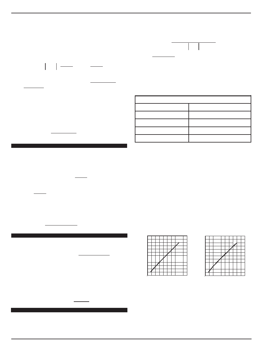
in the Electrical Characteristics Table. The charts below in
Figure 7 display curves of the fall time (90% - 10%) as a
function of the output load capacitance for both the 3V and
12V MAIN outputs.
0
200
400
600
800
1000
1200
0
5
00
0
5
0
5
100
150
200
250
LOAD
CAPACITANCE
(F)
FALL TIME (ms)
3V Output Discharge as a
Function of Load Capacitance
0
200
400
600
800
1000
1200
0
00
500 1000 1500 2000 2500
LOAD
CAPACITANCE
(F)
FALL TIME (ms)
12V Output Discharge as a
Function of Load Capacitance
Figure 7. 3V and 12V Output Discharge vs. Load
Capacitance
Standby Mode
Standby mode is entered when one or more of the MAIN
supply inputs (12VIN and/or 3VIN) is below its respective
UVLO threshold or OFF. The MIC2591B also supplies
3.3V auxiliary outputs (VAUX[A/B]), satisfying PCI Express
0.022F*
1.136V/ms
0.047F
0.532 V/ms
0.1F
0.250V/ms
dv/dt (load)
0.01F*
2.5V/ms
0.022F*
1.136V/ms
0.047F
0.532 V/ms
0.1F
0.250V/ms
相關(guān)PDF資料 |
PDF描述 |
|---|---|
| MIC30711-5100W-LF3 | 32 CONTACT(S), FEMALE, RIGHT ANGLE TELECOM AND DATACOM CONNECTOR, SOLDER |
| MIC3730-1.8BR | 1.8 V FIXED POSITIVE LDO REGULATOR, 0.5 V DROPOUT, PSSO5 |
| MIC5225-1.5YM5TR | 1.5 V FIXED POSITIVE LDO REGULATOR, 0.45 V DROPOUT, PDSO5 |
| MIC5225-2.5YM5TR | 2.5 V FIXED POSITIVE LDO REGULATOR, 0.45 V DROPOUT, PDSO5 |
| MIC5225-3.3YM5TR | 3.3 V FIXED POSITIVE LDO REGULATOR, 0.45 V DROPOUT, PDSO5 |
相關(guān)代理商/技術(shù)參數(shù) |
參數(shù)描述 |
|---|---|
| MIC2592B-2BTQ | 功能描述:IC CTRLR HOTPLUG PCI DUAL 48TQFP RoHS:否 類別:集成電路 (IC) >> PMIC - 熱交換 系列:- 產(chǎn)品培訓(xùn)模塊:Obsolescence Mitigation Program 標(biāo)準(zhǔn)包裝:100 系列:- 類型:熱插拔開關(guān) 應(yīng)用:通用 內(nèi)部開關(guān):是 電流限制:可調(diào) 電源電壓:9 V ~ 13.2 V 工作溫度:-40°C ~ 150°C 安裝類型:表面貼裝 封裝/外殼:10-WFDFN 裸露焊盤 供應(yīng)商設(shè)備封裝:10-TDFN-EP(3x3) 包裝:管件 |
| MIC2592B-2BTQ TR | 功能描述:IC PCI HOT PLUG CTLR DUAL 48TQFP RoHS:否 類別:集成電路 (IC) >> PMIC - 熱交換 系列:- 產(chǎn)品培訓(xùn)模塊:Obsolescence Mitigation Program 標(biāo)準(zhǔn)包裝:100 系列:- 類型:熱插拔開關(guān) 應(yīng)用:通用 內(nèi)部開關(guān):是 電流限制:可調(diào) 電源電壓:9 V ~ 13.2 V 工作溫度:-40°C ~ 150°C 安裝類型:表面貼裝 封裝/外殼:10-WFDFN 裸露焊盤 供應(yīng)商設(shè)備封裝:10-TDFN-EP(3x3) 包裝:管件 |
| MIC2592B-2YTQ | 功能描述:熱插拔功率分布 Dual-slot PCI-Express Hot Swap Power Controller - Lead Free RoHS:否 制造商:Texas Instruments 產(chǎn)品:Controllers & Switches 電流限制: 電源電壓-最大:7 V 電源電壓-最小:- 0.3 V 工作溫度范圍: 功率耗散: 安裝風(fēng)格:SMD/SMT 封裝 / 箱體:MSOP-8 封裝:Tube |
| MIC2592B-2YTQ TR | 功能描述:熱插拔功率分布 Dual-slot PCI-Express Hot Swap Power Controller - Lead Free RoHS:否 制造商:Texas Instruments 產(chǎn)品:Controllers & Switches 電流限制: 電源電壓-最大:7 V 電源電壓-最小:- 0.3 V 工作溫度范圍: 功率耗散: 安裝風(fēng)格:SMD/SMT 封裝 / 箱體:MSOP-8 封裝:Tube |
| MIC2593-2BTQ | 功能描述:IC CTRLR HOTPLUG PCI DUAL 48TQFP RoHS:否 類別:集成電路 (IC) >> PMIC - 熱交換 系列:- 產(chǎn)品培訓(xùn)模塊:Obsolescence Mitigation Program 標(biāo)準(zhǔn)包裝:100 系列:- 類型:熱插拔開關(guān) 應(yīng)用:通用 內(nèi)部開關(guān):是 電流限制:可調(diào) 電源電壓:9 V ~ 13.2 V 工作溫度:-40°C ~ 150°C 安裝類型:表面貼裝 封裝/外殼:10-WFDFN 裸露焊盤 供應(yīng)商設(shè)備封裝:10-TDFN-EP(3x3) 包裝:管件 |
發(fā)布緊急采購(gòu),3分鐘左右您將得到回復(fù)。