- 您現(xiàn)在的位置:買賣IC網(wǎng) > PDF目錄1954 > MCZ33781EKR2 (Freescale Semiconductor)IC MASTER DSI 2.02 DIFF 32-SOIC PDF資料下載
參數(shù)資料
| 型號(hào): | MCZ33781EKR2 |
| 廠商: | Freescale Semiconductor |
| 文件頁(yè)數(shù): | 9/44頁(yè) |
| 文件大?。?/td> | 0K |
| 描述: | IC MASTER DSI 2.02 DIFF 32-SOIC |
| 標(biāo)準(zhǔn)包裝: | 1,000 |
| 應(yīng)用: | 車載系統(tǒng) |
| 接口: | SPI |
| 電源電壓: | 4.75 V ~ 5.25 V |
| 封裝/外殼: | 32-BSOP(0.295",7.50mm 寬)裸露焊盤(pán) |
| 供應(yīng)商設(shè)備封裝: | 32-SOICW 裸露焊盤(pán) |
| 包裝: | 帶卷 (TR) |
| 安裝類型: | 表面貼裝 |
第1頁(yè)第2頁(yè)第3頁(yè)第4頁(yè)第5頁(yè)第6頁(yè)第7頁(yè)第8頁(yè)當(dāng)前第9頁(yè)第10頁(yè)第11頁(yè)第12頁(yè)第13頁(yè)第14頁(yè)第15頁(yè)第16頁(yè)第17頁(yè)第18頁(yè)第19頁(yè)第20頁(yè)第21頁(yè)第22頁(yè)第23頁(yè)第24頁(yè)第25頁(yè)第26頁(yè)第27頁(yè)第28頁(yè)第29頁(yè)第30頁(yè)第31頁(yè)第32頁(yè)第33頁(yè)第34頁(yè)第35頁(yè)第36頁(yè)第37頁(yè)第38頁(yè)第39頁(yè)第40頁(yè)第41頁(yè)第42頁(yè)第43頁(yè)第44頁(yè)
Analog Integrated Circuit Device Data
Freescale Semiconductor
17
33781
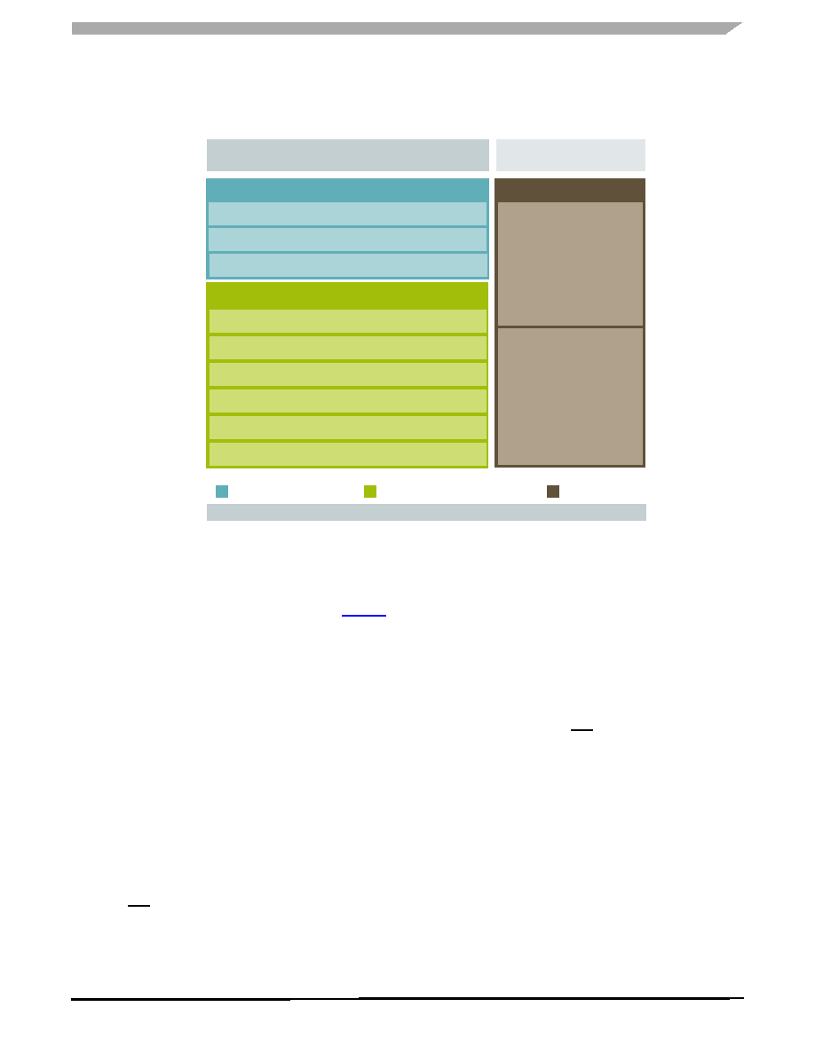
FUNCTIONAL DESCRIPTIONS
FUNCTIONAL INTERNAL BLOCK DESCRIPTION
FUNCTIONAL INTERNAL BLOCK DESCRIPTION
Figure 10. Block Illustration
The 33781 is controlled by an MCU through the SPI0
interface. It handles the digital and physical layer portions of
a DBUS master node. Four separate DBUS channels are
included. The physical layer uses a two-wire bus with analog
wave-shaped voltage and current signals. Refer to Figure 1.
Major subsystems include the following:
SPI0 interface and registers to a main MCU
SPI1 interface and registers to a second MCU
Four channels of DSI 2.02 protocol state logic
CRC block for each channel
Control and status registers
Four addressable register sets per channel for queuing up
to four commands and data per bus. The addressable
buffer acts as a circular buffer for command writes and
data reads.
Pseudo Bus Switch from D0H/L to DPH/L
SPI0 AND REGISTERS
This block contains the SPI0 interface logic and the control
and response registers that are written to and read from the
SPI interface.
The IC is an SPI slave-type device, so MOSI0 (Master-
Out-Slave-In) is an input and MISO0 (Master-In-Slave-Out) is
an output. CS0 and SCLK0 are also inputs.
The SPI0 port can handle 2-byte and 4-byte transfers. It
addresses 87 registers. The organization of the registers is
described in the section entitled SPI0 Register and Bit
SPI1 AND REGISTERS
The 33781 has a second SPI port (called SPI1) that allows
valid response data from Bus Channel 2 and 3, along with the
slave address, to be read independently by a second MCU.
This block contains the SPI1 interface logic and the response
registers that are read from the SPI1 interface.
The IC is an SPI slave-type device, so MISO1 (Master-In-
Slave-Out) is an output, and CS1 and SCLK1 are inputs. SPI1
does not use the MOSI (Master-Out-Slave-In) pin or function
as it does not receive commands.
The SPI1 port handles only 16-bit transfers. It addresses
eight registers which are read only.
PROTOCOL ENGINE
This block converts the data to be transmitted from the
registers into the DBUS sequences, and converts DBUS
response sequences to data in the registers.
The DBUS transmit protocol uses a return to 1 type data
with a duty cycle determined by the logic state. The protocol
includes Cyclical Redundancy Check (CRC) generation and
validation.
MC33781 - Functional Block Diagram
Supply Voltage
Power Stage
Supply Voltage
2.5V Regulator
Power Stage
CRC Generation and Checking
Clock Generation and Frequency Spreading
Logic and Control
Over-temperature Sensing
SPI0 Registers and State Machine
Over-current Sensing
DBUS Drivers
and Receivers
Pseudo-bus
Logic and Control
VSUP Voltage Monitor
HCAP Charging Circuitry
SPI1 Registers and State Machine
Switches
相關(guān)PDF資料 |
PDF描述 |
|---|---|
| MCZ33784EFR2 | IC SENSOR DBUS DSI 2.02 16-SOIC |
| MCZ33793EF | IC DSI SLAVE REMOTE SENS 16-SOIC |
| MCZ33797EKR2 | IC SQUIB DRIVER 2CHAN 32-SOIC |
| MCZ33884EG | IC MULTIPLE CONTACT MON 24-SOIC |
| MCZ33905BD3EK | IC SBC CAN HS 3.3V 54SOIC |
相關(guān)代理商/技術(shù)參數(shù) |
參數(shù)描述 |
|---|---|
| MCZ33784EF | 功能描述:加速計(jì) - 板上安裝 DBUS2 SENSOR INTERFACE RoHS:否 制造商:Murata 傳感軸:Double 加速:12 g 靈敏度: 封裝 / 箱體: 輸出類型:Analog 數(shù)字輸出 - 位數(shù):11 bit 電源電壓-最大:5.25 V 電源電壓-最小:4.75 V 電源電流:4 mA 最大工作溫度:+ 125 C 最小工作溫度:- 40 C |
| MCZ33784EF/R2- | 制造商:FREESCALE 制造商全稱:Freescale Semiconductor, Inc 功能描述:DSI 2.02 Sensor Interface |
| MCZ33784EFR2 | 功能描述:加速計(jì) - 板上安裝 DBUS2 SENSOR INTERFACE RoHS:否 制造商:Murata 傳感軸:Double 加速:12 g 靈敏度: 封裝 / 箱體: 輸出類型:Analog 數(shù)字輸出 - 位數(shù):11 bit 電源電壓-最大:5.25 V 電源電壓-最小:4.75 V 電源電流:4 mA 最大工作溫度:+ 125 C 最小工作溫度:- 40 C |
| MCZ33789AE | 功能描述:網(wǎng)絡(luò)控制器與處理器 IC Airbag ASSP RoHS:否 制造商:Micrel 產(chǎn)品:Controller Area Network (CAN) 收發(fā)器數(shù)量: 數(shù)據(jù)速率: 電源電流(最大值):595 mA 最大工作溫度:+ 85 C 安裝風(fēng)格:SMD/SMT 封裝 / 箱體:PBGA-400 封裝:Tray |
| MCZ33789AE/R2 | 制造商:FREESCALE 制造商全稱:Freescale Semiconductor, Inc 功能描述:Airbag System Basis Chip (SBC) with Power Supply and PSI5 Sensor Interface |
發(fā)布緊急采購(gòu),3分鐘左右您將得到回復(fù)。