- 您現(xiàn)在的位置:買賣IC網(wǎng) > PDF目錄299472 > MC74LCX00SD (ON SEMICONDUCTOR) 15 A 12-V Input Bus Termination Power Module for DDR/QDR Memory 10-DIP MODULE -40 to 85 PDF資料下載
參數(shù)資料
| 型號: | MC74LCX00SD |
| 廠商: | ON SEMICONDUCTOR |
| 元件分類: | 門電路 |
| 英文描述: | 15 A 12-V Input Bus Termination Power Module for DDR/QDR Memory 10-DIP MODULE -40 to 85 |
| 中文描述: | LVC/LCX/Z SERIES, QUAD 2-INPUT NAND GATE, PDSO14 |
| 封裝: | PLASTIC, SSOP-14 |
| 文件頁數(shù): | 9/40頁 |
| 文件大?。?/td> | 350K |
| 代理商: | MC74LCX00SD |
第1頁第2頁第3頁第4頁第5頁第6頁第7頁第8頁當(dāng)前第9頁第10頁第11頁第12頁第13頁第14頁第15頁第16頁第17頁第18頁第19頁第20頁第21頁第22頁第23頁第24頁第25頁第26頁第27頁第28頁第29頁第30頁第31頁第32頁第33頁第34頁第35頁第36頁第37頁第38頁第39頁第40頁
LCX Family Characteristics
LCX DATA
BR1339 — REV 3
15
MOTOROLA
LCX — Low–Voltage CMOS Logic (WIth
5V–Tolerant Inputs and Outputs)
The LCX family represents Motorola’s Low–Voltage
CMOS family. These devices offer mixed 3V–5V capability
and are recommended for applications where 3.3V and 5V
subsystems interface with one another and where low power
consumption is a necessity. The input and output (Note 1)
structures of the LCX family of products will tolerate input and
output node exposure to signals or DC levels that exceed the
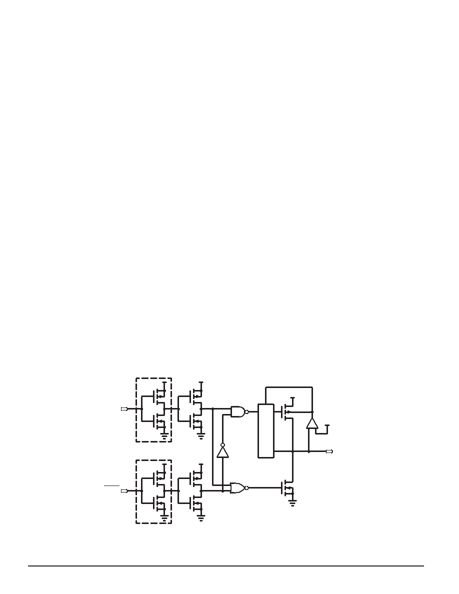
VCC level (Note 2). Refer to Figure 11 for schematic
description of a typical LCX circuit. Note that the output
PMOS device P1 has its bulk potential supplied by the output
of the comparator X1 rather than by VCC as in conventional
CMOS. The circuitry contained within the comparator is
designed such that the output is always the greater of VCC or
VO. This technique circumvents the P+/N– bulk–source
forward junction that usually appears between the PMOS
drain at the output and the bulk connection of the output
PMOS which is usually tied to VCC. Eliminating this junction is
fundamental to the powered–down high Z and overvoltage
tolerance features that distinguish Motorola’s LCX family
from other Low–Voltage CMOS products.
NOTE 1: U.S. Patent 5,451,889.
NOTE 2: Output overvoltage is permitted unconditionally for 3–stated outputs.
For active outputs, see datasheet.
LVX-Low Voltage Dual Supply Translating
Transceivers
In applications where 3.3V signals must be “stepped up” to
5V, in order to interface full swing CMOS busses, LCX may
not be the proper solution. The LVX translating transceiver
designs have an entirely different approach to solve the
mixed supply interface problem. These devices are not
overvoltage tolerant, but rather true voltage translators —
meaning that they receive 3V signals and output 5V signals,
and receive 5V signals and output 3V signals (which can also
be accomplished with LCX). This is done by dividing the
devices internally so that the A–side circuitry is isolated from
the B–side circuitry. The dual supply architecture allows the
LVX translators to interface 3V and 5V signals with near–zero
static power dissipation.
The MC74LVX4245 A–side is dedicated to 5V operation,
with VCCA specified over the 4.5V–5.5V range. The B–side is
dedicated to 3.3V, with VCCB specified over the 2.7V–3.6V
range.
The MC74LVXC3245 offers enhanced interfacing
features. The B–side is designed to operate over an
extended range of I/O and supply levels. The VCCB is
permitted to be set to any value between 2.7V and 5.5V. The
I/O levels on the B–side will track or scale automatically
according to the level set on VCCB. The B–side operation is
completely independent of VCCA. The A–port and control
input buffers are referenced to VCCA, totally independent of
VCCB. The configurable dual supply translating transceiver,
LVXC3245, is designed to tolerate floating inputs on the
B–port when VCCA and the control signals are set to valid
operating levels. The combination of this on–the–fly interface
flexibility together with “empty socket” tolerance is intended
to benefit designers of PC card systems (or PCMCIA) where
expansion cards with different supply potentials must be
accommodated.
The LVX dual supply translators offer switching speeds
equivalent to 5V FCT/FAST but with low ground noise and
very low power dissipation.
Data
Enable
Input Stage
P1
X1
Output
VDD
VCC
Figure 11. Simplified LCX Schematic Diagram
相關(guān)PDF資料 |
PDF描述 |
|---|---|
| MC74LCX02D | 15 A 12-V Input Bus Termination Power Module for DDR/QDR Memory 10-DIP MODULE -40 to 85 |
| MC74LCX02M | 0.8 to 1.8 V 18-A, 12-V Input Non-Isolated Wide-Adjust Module 10-DIP MODULE -40 to 85 |
| MC74LCX02 | 15 A 12-V Input Bus Termination Power Module for DDR/QDR Memory 10-DIP MODULE -40 to 85 |
| MC74LCX540DWR2 | LVC/LCX/Z SERIES, 8-BIT DRIVER, INVERTED OUTPUT, PDSO20 |
| MC74LCX646DTR2 | LVC/LCX/Z SERIES, 8-BIT REGISTERED TRANSCEIVER, TRUE OUTPUT, PDSO24 |
相關(guān)代理商/技術(shù)參數(shù) |
參數(shù)描述 |
|---|---|
| MC74LCX02D | 功能描述:邏輯門 2-3.6V Quad 2-Input RoHS:否 制造商:Texas Instruments 產(chǎn)品:OR 邏輯系列:LVC 柵極數(shù)量:2 線路數(shù)量(輸入/輸出):2 / 1 高電平輸出電流:- 16 mA 低電平輸出電流:16 mA 傳播延遲時間:3.8 ns 電源電壓-最大:5.5 V 電源電壓-最小:1.65 V 最大工作溫度:+ 125 C 安裝風(fēng)格:SMD/SMT 封裝 / 箱體:DCU-8 封裝:Reel |
| MC74LCX02DG | 功能描述:邏輯門 2-3.6V Quad 2-Input NOR RoHS:否 制造商:Texas Instruments 產(chǎn)品:OR 邏輯系列:LVC 柵極數(shù)量:2 線路數(shù)量(輸入/輸出):2 / 1 高電平輸出電流:- 16 mA 低電平輸出電流:16 mA 傳播延遲時間:3.8 ns 電源電壓-最大:5.5 V 電源電壓-最小:1.65 V 最大工作溫度:+ 125 C 安裝風(fēng)格:SMD/SMT 封裝 / 箱體:DCU-8 封裝:Reel |
| MC74LCX02DR2 | 功能描述:邏輯門 2-3.6V Quad 2-Input RoHS:否 制造商:Texas Instruments 產(chǎn)品:OR 邏輯系列:LVC 柵極數(shù)量:2 線路數(shù)量(輸入/輸出):2 / 1 高電平輸出電流:- 16 mA 低電平輸出電流:16 mA 傳播延遲時間:3.8 ns 電源電壓-最大:5.5 V 電源電壓-最小:1.65 V 最大工作溫度:+ 125 C 安裝風(fēng)格:SMD/SMT 封裝 / 箱體:DCU-8 封裝:Reel |
| MC74LCX02DR2G | 功能描述:邏輯門 2-3.6V Quad 2-Input NOR RoHS:否 制造商:Texas Instruments 產(chǎn)品:OR 邏輯系列:LVC 柵極數(shù)量:2 線路數(shù)量(輸入/輸出):2 / 1 高電平輸出電流:- 16 mA 低電平輸出電流:16 mA 傳播延遲時間:3.8 ns 電源電壓-最大:5.5 V 電源電壓-最小:1.65 V 最大工作溫度:+ 125 C 安裝風(fēng)格:SMD/SMT 封裝 / 箱體:DCU-8 封裝:Reel |
| MC74LCX02DT | 功能描述:邏輯門 2-3.6V Quad 2-Input RoHS:否 制造商:Texas Instruments 產(chǎn)品:OR 邏輯系列:LVC 柵極數(shù)量:2 線路數(shù)量(輸入/輸出):2 / 1 高電平輸出電流:- 16 mA 低電平輸出電流:16 mA 傳播延遲時間:3.8 ns 電源電壓-最大:5.5 V 電源電壓-最小:1.65 V 最大工作溫度:+ 125 C 安裝風(fēng)格:SMD/SMT 封裝 / 箱體:DCU-8 封裝:Reel |
發(fā)布緊急采購,3分鐘左右您將得到回復(fù)。