- 您現(xiàn)在的位置:買賣IC網(wǎng) > PDF目錄370849 > M37753FFCHP (Mitsubishi Electric Corporation) SINGLE CHIP 16 BIT CMOS MICROCOMPUTER FLASH MEMORY VERSION PDF資料下載
參數(shù)資料
| 型號(hào): | M37753FFCHP |
| 廠商: | Mitsubishi Electric Corporation |
| 英文描述: | SINGLE CHIP 16 BIT CMOS MICROCOMPUTER FLASH MEMORY VERSION |
| 中文描述: | 單片微機(jī)16位CMOS閃存版 |
| 文件頁(yè)數(shù): | 32/67頁(yè) |
| 文件大小: | 525K |
| 代理商: | M37753FFCHP |
第1頁(yè)第2頁(yè)第3頁(yè)第4頁(yè)第5頁(yè)第6頁(yè)第7頁(yè)第8頁(yè)第9頁(yè)第10頁(yè)第11頁(yè)第12頁(yè)第13頁(yè)第14頁(yè)第15頁(yè)第16頁(yè)第17頁(yè)第18頁(yè)第19頁(yè)第20頁(yè)第21頁(yè)第22頁(yè)第23頁(yè)第24頁(yè)第25頁(yè)第26頁(yè)第27頁(yè)第28頁(yè)第29頁(yè)第30頁(yè)第31頁(yè)當(dāng)前第32頁(yè)第33頁(yè)第34頁(yè)第35頁(yè)第36頁(yè)第37頁(yè)第38頁(yè)第39頁(yè)第40頁(yè)第41頁(yè)第42頁(yè)第43頁(yè)第44頁(yè)第45頁(yè)第46頁(yè)第47頁(yè)第48頁(yè)第49頁(yè)第50頁(yè)第51頁(yè)第52頁(yè)第53頁(yè)第54頁(yè)第55頁(yè)第56頁(yè)第57頁(yè)第58頁(yè)第59頁(yè)第60頁(yè)第61頁(yè)第62頁(yè)第63頁(yè)第64頁(yè)第65頁(yè)第66頁(yè)第67頁(yè)
32
PRELIMINARY
Notice: This is not a final specification.
Some parametric limits are subject to change.
MITSUBISHI MICROCOMPUTERS
M37753FFCFP
M37753FFCHP
SHINGLE-CHIP 16-BIT CMOS MICROCOMPUTER FLASH MEMORY VERSION
CPU reprogramming mode operation proce-
dure
The operation procedure in CPU reprogramming mode is described
below.
< Beginning procedure >
Apply 0 V to the CNVss/V
PP
pin for reset release.
Set the processor mode register 0 (see Figure 23).
After CPU reprogramming mode control program is transferred to
internal RAM, jump to this control program on RAM. (The follow-
ing operations are controlled by this control program).
Set “1" (8-bit length) to data length select flag m.
Set “1" to the CPU reprogramming mode select bit.
Apply V
PP
H to the CNV
SS
/V
PP
pin.
Read the CPU reprogramming mode monitor flag to confirm
whether the CPU reprogramming mode is valid.
The operation of the flash memory is executed by software-com-
mand-writing to the flash command register .
Note:
The following are necessary other than this:
Control for data which is input from the external (serial I/O
etc.) and to be programmed to the flash memory
Initial setting for ports etc.
Writing to the watchdog timer
< Release procedure >
Apply 0V to the CNV
SS
/V
PP
pin.
Set the CPU reprogramming mode select bit to “0.”
Each software command is explained as follows.
Read command
When “00
16
" is written to the flash command register, the
M37753FFCFP and the M37753FFCHP enter the read mode. The
contents of the corresponding address can be read by reading the
flash memory (For instance, with the LDA instruction etc.) under this
condition.
The read mode is maintained until another command code is written
to the flash command register. Accordingly, after setting the read
mode once, the contents of the flash memory can continuously be
read.
After reset and after the reset command is executed, the read mode
is set.
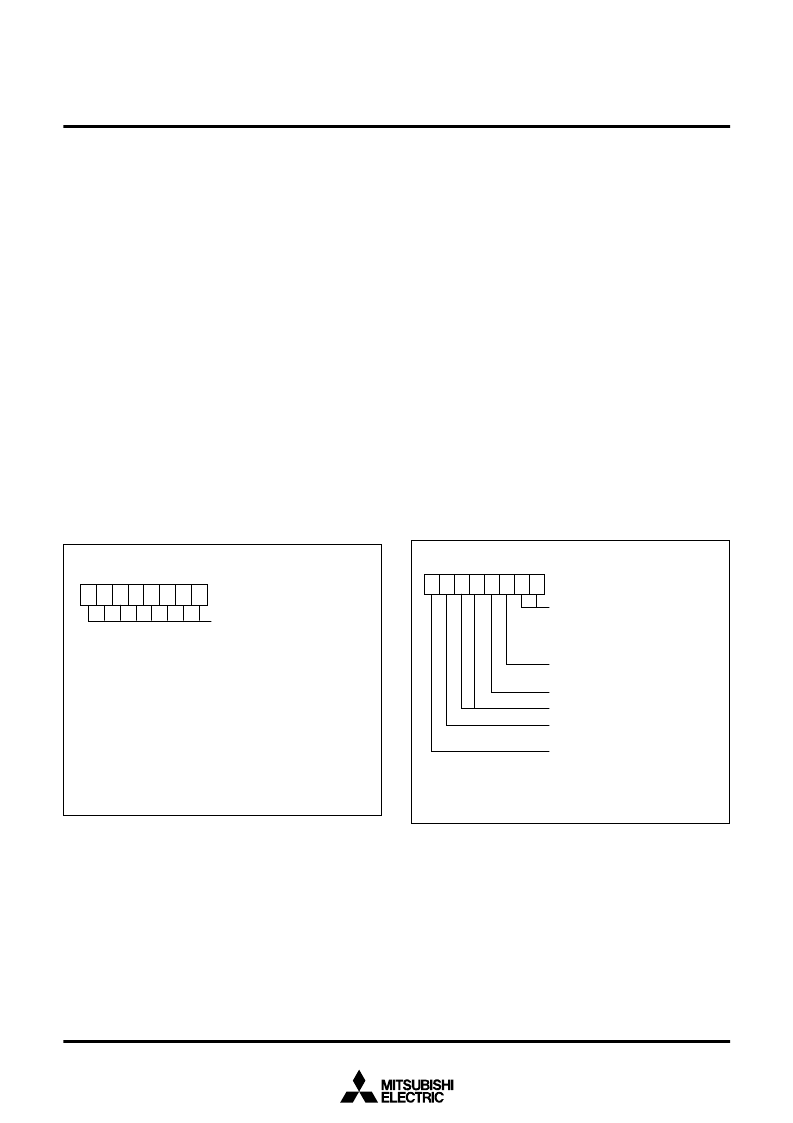
Fig. 22 Flash command register bit configuration
Writing of software command
<Command code>
“00
16
”
“40
16
”
“C0
16
”
“20
16
” + “20
16
”
“A0
16
”
“30
16
” + “30
16
”
“FF
16
” + “FF
16
”
<Software command name>
Read command
Program command
Program verify command
Erase command
Erase verify command
Auto erase command
Reset command
Note:
The flash command register is write-only register.
Flash command register
Address
65
16
7
6
5
4
3
2
1
0
7
6
5
4
3
2
1
0
0
0
0
Processor mode register 0
Internal memory access bus cycle select bit
Fix this bit to “0.”
Software reset bit
Interrupt priority detection time select bits
Clock
φ
1
output select bit
Test mode bit
Fix this bit to “0.”
Processor mode bits
0 0 : Single-chip mode
0 1 : Memory expansion mode
1
: Do not select.
Note:
For the description of processor mode register 0, refer to Figure 14
on the M37754M8C-XXXGP data sheet.
Address
5E
16
Fig. 23 Processor mode register 0 bit configuration in CPU rewrit-
ing mode
相關(guān)PDF資料 |
PDF描述 |
|---|---|
| M37754M8C-XXXGP | SINGLE-CHIP 16BIT CMOS MICROCOMPUTER |
| M37754M8C-XXXHP | SINGLE-CHIP 16BIT CMOS MICROCOMPUTER |
| M37754S4CGP | SINGLE-CHIP 16BIT CMOS MICROCOMPUTER |
| M37754S4CHP | SINGLE-CHIP 16BIT CMOS MICROCOMPUTER |
| M37754 | SINGLE-CHIP 16BIT CMOS MICROCOMPUTER |
相關(guān)代理商/技術(shù)參數(shù) |
參數(shù)描述 |
|---|---|
| M37753M6C-XXXFP | 制造商:RENESAS 制造商全稱:Renesas Technology Corp 功能描述:SINGLE-CHIP 16-BIT CMOS MICROCOMPUTER |
| M37753M6C-XXXHP | 制造商:RENESAS 制造商全稱:Renesas Technology Corp 功能描述:SINGLE-CHIP 16-BIT CMOS MICROCOMPUTER |
| M37753M8C-XXXFP | 制造商:RENESAS 制造商全稱:Renesas Technology Corp 功能描述:SINGLE-CHIP 16-BIT CMOS MICROCOMPUTER |
| M37753M8C-XXXHP | 制造商:RENESAS 制造商全稱:Renesas Technology Corp 功能描述:SINGLE-CHIP 16-BIT CMOS MICROCOMPUTER |
| M37753S4CFP | 制造商:RENESAS 制造商全稱:Renesas Technology Corp 功能描述:SINGLE-CHIP 16-BIT CMOS MICROCOMPUTER |
發(fā)布緊急采購(gòu),3分鐘左右您將得到回復(fù)。